

L298N Dual Full Bridge Driver IC Multiwatt-15 Package

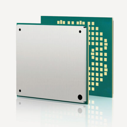
L30960-N3400-A400
Features of L30960-N3400-A400
- LTE (20,8,3,7,1); 3G (8,3); and 2G Dual Band PLS8-E
- PLS8-US: 3G (5,4,2), 2G Quad Band, and LTE (17,5,4,2).
- LTE (1,3,19); 3G; PLS8-J (1,19)
- PLS8-X: 3G (5,4,2), 2G Quad Band, and LTE (13,17,5,4,2).
- LTE PLS8-V: (13,4,2)
- LTE (2x2 DL-MIMO; FDD 3GPP Release 9)
- 3GPP Release 8; UMTS/HSPA (FDD); Rx diversity
- 3GPP Release 6; DARP/SAIC; GSM/GPRS/EDGE
- SIM Application Toolkit, version 99 of the 3GPP
- Using AT instructions to control (Hayes, TS 27.007, TS 27.005)
- Complete GPS/GLONASS integration (Qualcomm gpsOne Gen8A)
- 3.3 to 4.2 V supply voltage range, especially tuned for low power usage
- Dimensions are 29 mm by 33 mm by 2,2 mm (PLS8-V/-X: H=2,9 mm).
- Range of Operation: -40 ?C to +85 ?C
- EuP support, RoHS and REACH compliance
- Multiple composite modes and a Linux/Mac-compliant mode are supported by the USB interface.
- USB-based firmware update
- BIP (Bearer Independent Protocol) (Bearer Independent Protocol)
- From Rel.3.0 and for PLS8-X /-V, IP services (Client & Server, TCP/IP & UDP, Transparent & Nontransparent) are available.
- According to 3GPP TS 27.010, a multiplexer
- Carrier Switching Automatic (PLS8-X)
L30960-N3410-A400
Features of L30960-N3410-A400
- LTE (20,8,3,7,1); 3G (8,3); and 2G Dual Band PLS8-E
- PLS8-US: 3G (5,4,2), 2G Quad Band, and LTE (17,5,4,2).
- LTE (1,3,19); 3G; PLS8-J (1,19)
- PLS8-X: 3G (5,4,2), 2G Quad Band, and LTE (13,17,5,4,2).
- LTE PLS8-V: (13,4,2)
- LTE (2x2 DL-MIMO; FDD 3GPP Release 9)
- 3GPP Release 8; UMTS/HSPA (FDD); Rx diversity
- 3GPP Release 6; DARP/SAIC; GSM/GPRS/EDGE
- SIM Application Toolkit, version 99 of the 3GPP
- Using AT instructions to control (Hayes, TS 27.007, TS 27.005)
- Complete GPS/GLONASS integration (Qualcomm gpsOne Gen8A)
- 3.3 to 4.2 V supply voltage range, especially tuned for low power usage
- Dimensions are 29 mm by 33 mm by 2,2 mm (PLS8-V/-X: H=2,9 mm).
- Range of Operation: -40 ?C to +85 ?C
- EuP support, RoHS and REACH compliance
- Multiple composite modes and a Linux/Mac-compliant mode are supported by the USB interface.
- USB-based firmware update
- BIP (Bearer Independent Protocol) (Bearer Independent Protocol)
- From Rel.3.0 and for PLS8-X /-V, IP services (Client & Server, TCP/IP & UDP, Transparent & Nontransparent) are available.
- According to 3GPP TS 27.010, a multiplexer
- PLS8-X Automatic Carrier Switching

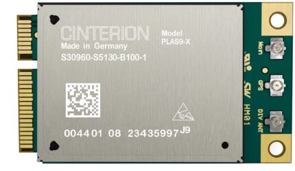
L30960-N5130-B100
Features? of? L30960-N5130-B100
- LTE (2x2 DL-MIMO; FDD 3GPP Release 9)
- 3GPP Release 8; UMTS/HSPA (FDD); Rx diversity
- 3GPP Release 6; DARP/SAIC; GSM/GPRS/EDGE
- SIM Application Toolkit, version 99 of the 3GPP
- Using AT instructions to control (Hayes, TS 27.007, TS 27.005)
- 3.3 to 4.2 V supply voltage range, especially tuned for low power usage
- Size: 40, 32, and 2,8 mm
- Range of Operation Temperature: -40 ?C to +95 ?
- Compliant with RoHS, RED, and REACH, EuP assistance
- The USB 2.0/3.0 interface provides several composite modes and a mode that is compatible with Linux and Mac.
- USB-based firmware update


L4970A
The L4970A is a stepdown monolithic power
switching regulator delivering 10A at a voltage
variable from 5.1 to 40V.
Realized with BCD mixed technology, the device
uses a DMOS output transistor to obtain very high
efficiency and very fast switching times. Features
of the L4970A include reset and power fail for microprocessors, feed forward line regulation, soft
start, limiting current and thermal protection. The
device is mounted in a 15-lead multiwatt plastic
power package and requires few external components. Efficient operation at switching frequencies
up to 500KHz allows reduction in the size and
cost of external filter components.
L4978D
The L4978 is a step down monolithic power
switching regulator delivering 2A at a voltage between 3.3V and 50V (selected by a simple external
divider). Realized in BCD mixed technology, the
device uses an internal power D-MOS transistor
(with a typical Rdson of 0.25?) to obtain very high
efficency and high switching speed
L6201
The I.C. is a full bridge driver for motor control applications realized in Multipower-BCD technology
which combines isolated DMOS power transistors
with CMOS and Bipolar circuits on the same chip.
By using mixed technology it has been possible to
optimize the logic circuitry and the power stage to
achieve the best possible performance. The
DMOS output transistors can operate at supply
voltages up to 42V and efficiently at high switching speeds. All the logic inputs are TTL, CMOS
and ?C compatible. Each channel (half-bridge) of
the device is controlled by a separate logic input,
while a common enable controls both channels.
The I.C. is mounted in three different packages.


