AD549AJH
The AD549 is a low-input bias current monolithic electrometer operational amplifier. For accurate performance, input offset voltage and input offset voltage drift are laser trimmed. TopgateTM JFET technology, a process development only used by Analog Devices, Inc., is used to achieve the part's ultralow input current. This approach enables the manufacturing of JFETs with extremely low input currents that are compatible with a standard connection isolated bipolar process. The bootstrapped input stage's 1015 common-mode impedance ensures that the input current is entirely independent of the common mode voltage. The AD549 is ideal for applications that require very low input current and very low input offset voltage. It performs admirably as a preamp for a wide range of current output transducers, including photodiodes, photomultiplier tubes, and oxygen sensors. The AD549 can also be utilized as a precision integrator or a sample-and-hold with low droop. The AD549 is pin compatible with ordinary FET and electrometer op amps, enabling designers to improve the performance of existing systems at a cheap cost. The AD549 is supplied in a hermetic TO-99 package. Because the metal casing is linked to Pin 8, it can be independently connected to a point at the same voltage as the input terminals, eliminating stray leakage to the case. The AD549 is offered in four different performance levels. The J, K, and L models are rated for commercial temperatures ranging from 0°C to 70°C. The S grade is specified for military temperatures ranging from 55°C to 125°C and is available in MIL-STD-883B, Rev. C processing. Screening and extended reliability are other options. In addition, screening comprises a 168-hour burn-in period as well as various environmental and physical testing based on MIL-STD-883B, Rev. C.
AD7789BRMZ
The AD7788/AD7789 are analogue front ends with minimal power and noise for low frequency measuring applications. The AD7789 has a low noise, 24-bit analog-to-digital converter (ADC) with one differential input. The AD7788 is the 16-bit counterpart of the AD7789. The gadgets run on an internal clock. As a result, the user is not required to give a clock source to the devices. The output data rate is 16.6 Hz, resulting in concurrent 50 Hz/60 Hz rejection. The devices are powered by a single 2.5 V to 5.25 V power source. The maximum power dissipation for the gadget when powered by a 3 V supply is 225 W. The AD7788/AD7789 are offered in a 10-lead MSOP configuration.
APPLICATIONS
Intelligent transmitters
Applications for batteries
Instrumentation that is portable
Sensor evaluation
Temperature reading
Measurement of pressure
Weigh scales ranging from 4 to 20 mA circuits

ADM 485 JRZ
Meets EIA RS-485 standard
5 Mbps data rate
Single 5 V supply
–7 V to 12 V bus common-mode range
High speed, low power BiCMOS
Thermal shutdown protection
Short-circuit protection
Driver propagation delay: 10 ns typical
Receiver propagation delay: 15 ns typical
High-Z outputs with power off
Superior upgrade for LTC485
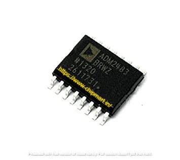
ADM2483BRWZ
The ADM2483 differential bus transceiver is a galvanically separated integrated component designed for bidirectional data transfer over balanced multipoint bus transmission lines.
It meets ANSI EIA/TIA-485-A and ISO 8482: 1987 standards (E).
The ADM2483 combines a 3-channel isolator, a three-state differential line driver, and a differential input receiver into a single device using Analog Devices, Inc.'s iCoupler technology.
The logic side of the device is powered by either a 5 V or 3 V source, while the bus side is supplied only by a 5 V supply.
To prevent reflections caused by poorly terminated transmission lines, the ADM2483 is slew-limited. The data rate is limited to 500 kbps due to the restricted slew rate. The input impedance of the device is 96 k, enabling up to 256 transceivers on the bus.
Internally, the driver differential outputs and receiver differential inputs comprise a differential input/output (I/O) port.
When the driver is deactivated or VDD1 or VDD2 = 0 V, the bus is under minimum load. There is also an active-high receiver disable function, which forces the receive output to enter a high impedance condition.
When the receiver inputs are open or shorted, a real fail-safe feature provides a logic-high receiver output level. This ensures that the receiver outputs are in a known condition before and after communication begins and terminates.


