Showing 1–12 of 1714 results

25RIA120

1,540.00
? Improved glass passivation for high reliability and exceptional stability at high temperature ? High dI/dt and dV/dt capabilities ? Standard package ? Low thermal resistance ? Metric threads version available ? Types up to 1200 V VDRM/VRRM ? Designed and qualified for industrial and consumer level

3296Y-1-502LF

215.00
Multiturn / Cermet / Industrial / Sealed 5 terminal styles Tape and reel packaging available Chevron seal design Listed on the QPL for style RJ24 per MIL-R-22097 and RJR24 per High-Rel Mil-R-39035 Mounting hardware available (H-117P) n RoHS compliant* version availabl

74F74N

49.00
These devices contain two independent positiveedge-triggered D-type flip-flops. A low level at the preset (PRE) or clear (CLR) inputs sets or resets the outputs regardless of the levels of the other inputs. When PRE and CLR are inactive (high), data at the data (D) input meeting the setup time requirements is transferred to the outputs on the positive-going edge of the clock pulse. Clock triggering occurs at a voltage level and is not directly related to the rise time of the clock pulse. Following the hold-time interval, data at the D input may be changed without affecting the levels at the outputs.
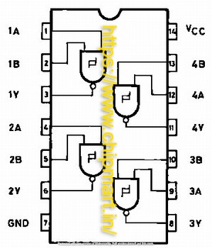
74HC132

45.00
Features ? Buffering of inputs ? Wide working temperature range: -40?C to 85?C ?Fanout up to 10 LSTTL loads ? Significant power savings over LSTTL logic ICs Application
  • Used to make alarm/tamper detect circuit
  • S-R latch
Description This gadget has four separate 2-input NAND gates. In positive logic, each gate executes the Boolean function Y = A B. There are balanced CMOS push-pull outputs on this chip. The word "balanced" refers to the device's ability to sink and source equivalent currents. This device's drive capabilities may result in quick edges into mild loads, hence routing and load circumstances should be examined to avoid ringing. Furthermore, the device's outputs are capable of pushing higher currents than the device can withstand without being harmed. It is critical that the device's output power be restricted to avoid overcurrent damage. At all times, the electrical and thermal limitations established in the Absolute Maximum Ratings must be observed. Push-pull CMOS outputs that are not in use should be unplugged.

74LS76 Dual JK Flip-Flop with Set and Clear IC7476

60.00

IC7476 jk flip flop

SN7476?is a?dual in-line JK flip flop IC, i.e. it has two JK flip flops inside it and each can be used individually based on our application. The term JK flip flop comes after its inventor Jack Kilby. The JK flip flops are considered to be the most efficient flip-flop and can be used for certain applications on its own. The flip-flops are also called as latching devices meaning it can remember one single bit of data and latch the output based on it, due to this property they are commonly used as shift registers, control registers, storage registers or where ever a small memory is required. More than one Flip Flop can be used in series to act as an EEPROM for holding small amount of data. The JK flip flop is considered to be more suitable for practical application because of its truth table that is the output of the flip flop will be stable for all types of inputs. 7476 IC Datasheet