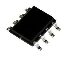
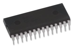
TL072C
? High slew rate: 20 V/?s (TL07xH, typ)
? Low offset voltage: 1 mV (TL07xH, typ)
? Low offset voltage drift: 2 ?V/?C
? Low power consumption: 940 ?A/ch (TL07xH, typ)
? Wide common-mode and differential
voltage ranges
? Common-mode input voltage range
includes VCC
? Low input bias and offset currents
? Low noise:
Vn = 18 nV/?Hz (typ) at f = 1 kHz
? Output short-circuit protection
? Low total harmonic distortion: 0.003% (typ)
? Wide supply voltage:
?2.25 V to ?20 V, 4.5 V to 40 V
TL082CD
The TL082, TL082A and TL082B are high speed
JFET input dual operational amplifiers
incorporating well-matched, high voltage JFET
and bipolar transistors in a monolithic integrated
circuit.
The devices feature high slew rates, low input
bias and offset current, and low offset voltage
temperature coefficient.
TL084C
The TL084, TL084A, and TL084B are high-speed,
JFET input, quad operational amplifiers
incorporating well matched, high voltage JFET
and bipolar transistors in a monolithic integrated
circuit.
The devices feature high slew rates, low input
bias and offset currents, and low offset voltage
temperature coefficient
TL16C550CPT
The TL16C550C and the TL16C550CI are
functional upgrades of the TL16C550B asynchronous
communications element (ACE), which in turn is a
functional upgrade of the TL16C450. Functionally
equivalent to the TL16C450 on power up (character
or TL16C450 mode), the TL16C550C and the
TL16C550CI, like the TL16C550B, can be placed
in an alternate FIFO mode. This relieves the
CPU of excessive software overhead by buffering
received and transmitted characters. The receiver
and transmitter FIFOs store up to 16 bytes including
three additional bits of error status per byte for the
receiver FIFO. In the FIFO mode, there is a selectable
autoflow control feature that can significantly reduce
software overload and increase system efficiency by
automatically controlling serial data flow using RTS
output and CTS input signals
TL431CD
The TL431 and TL432 devices are three-terminal
adjustable shunt regulators, with specified thermal
stability over applicable automotive, commercial, and
military temperature ranges. The output voltage can
be set to any value between Vref (approximately
2.5 V) and 36 V, with two external resistors. These
devices have a typical output impedance of 0.2 ?.
Active output circuitry provides a very sharp turn-on
characteristic, making these devices excellent
replacements for Zener diodes in many applications,
such as onboard regulation, adjustable power
supplies, and switching power supplies. The TL432
device has exactly the same functionality and
electrical specifications as the TL431 device, but has
different pinouts for the DBV, DBZ, and PK packages
TL497ACN
The TL497A incorporates all the active functions required in the construction of switching voltage regulators.
It also can be used as the control element to drive external components for high-power-output applications. The
TL497A was designed for ease of use in step-up, step-down, or voltage-inversion applications requiring high
efficiency
TL7705ACD
TL7757CD
The TL7757 is a supply-voltage supervisor
designed for use in microcomputer and
microprocessor systems. The supervisor
monitors the supply voltage for undervoltage
conditions. During power up, when the supply
voltage, VCC, attains a value approaching 1 V, the
RESET output becomes active (low) to prevent
undefined operation. If the supply voltage drops
below threshold voltage level (VIT?), the RESET
output goes to the active (low) level until the
supply undervoltage fault condition is eliminated.
TLC2274CN
1? Output Swing Includes Both Supply Rails
? Low Noise: 9 nV/?Hz Typical at f = 1 kHz
? Low-Input Bias Current: 1-pA Typical
? Fully-Specified for Both Single-Supply and SplitSupply Operation
? Common-Mode Input Voltage Range Includes
Negative Rail
? High-Gain Bandwidth: 2.2-MHz Typical
? High Slew Rate: 3.6-V/?s Typical
? Low Input Offset Voltage: 950 ?V Maximum at
TA = 25?C
? Macromodel Included
? Performance Upgrades for the TLC272 and
TLC274
? Available in Q-Temp Automotive


