
CD4007 Dual Complementary Pair with Inverter IC DIP-14 Package


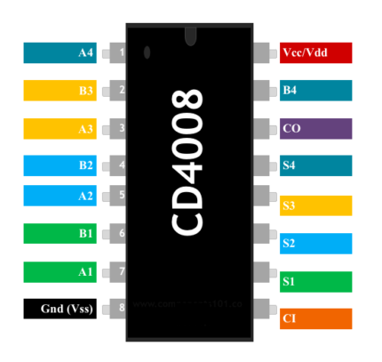

CD4008 4-bit Full Adder IC DIP-16 Package
CD4009 CMOS Hex Buffers/Converter IC DIP-16 Package
CD4010 Hex Buffer/Converter IC DIP-16 Package


CD40106 Hex Schmitt Trigger Inverter IC DIP-14 Package
CD40109 CMOS Quad Low-to-High Voltage Level Shifter IC DIP-16 Package


