AD5316ARUZ
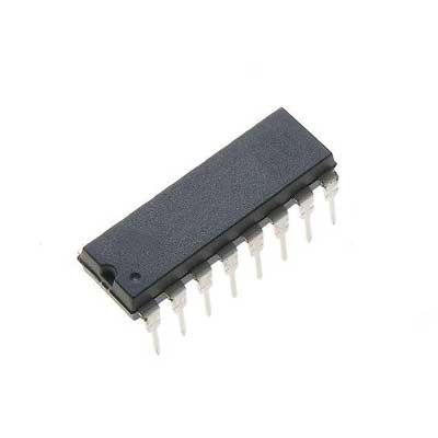
The AD5306/AD5316/AD53261
are quad 8-/10-/12-bit buffered
voltage output DACs in 16-lead TSSOP packages that operate
from a single 2.5 V to 5.5 V supply, consuming 500 ?A at 3 V.
Their on-chip output amplifiers allow rail-to-rail output swing
with a slew rate of 0.7 V/?s. A 2-wire serial interface, which
operates at clock rates up to 400 kHz, is used. This interface is
SMBus-compatible at VDD < 3.6 V. Multiple devices can be
placed on the same bus.
AD536AJH
The AD536A is a complete monolithic integrated circuit that performs the true RMS-to-dc conversion. It offers performance comparable to or superior to that of hybrid or modular units costing much more. The AD536A directly computes the true RMS value of any complex input waveform containing ac and dc components.
Mfr. No: AD536AJH
Mfr.:Analog Devices
Description: Power Management Specialised - PMIC RMS/DC CONVERTER IC
Datasheet: AD536AJH Datasheet (PDF)
AD538AD
The AD538 is a monolithic real-time computational circuit
that provides precision analog multiplication, division, and
exponentiation. The combination of low input and output offset
voltages and excellent linearity results in accurate computation
over an unusually wide input dynamic range. Laser wafer
trimming makes multiplication and division with errors as low
as 0.25% of reading possible, while typical output offsets of
100 ?V or less add to the overall off-the-shelf performance level.
Real-time analog signal processing is further enhanced by the
400 kHz bandwidth of the device.
AD549AJH
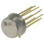
The AD549 is a low-input bias current monolithic electrometer operational amplifier. For accurate performance, input offset voltage and input offset voltage drift are laser trimmed. TopgateTM JFET technology, a process development only used by Analog Devices, Inc., is used to achieve the part's ultralow input current. This approach enables the manufacturing of JFETs with extremely low input currents that are compatible with a standard connection isolated bipolar process. The bootstrapped input stage's 1015 common-mode impedance ensures that the input current is entirely independent of the common mode voltage. The AD549 is ideal for applications that require very low input current and very low input offset voltage. It performs admirably as a preamp for a wide range of current output transducers, including photodiodes, photomultiplier tubes, and oxygen sensors. The AD549 can also be utilized as a precision integrator or a sample-and-hold with low droop. The AD549 is pin compatible with ordinary FET and electrometer op amps, enabling designers to improve the performance of existing systems at a cheap cost. The AD549 is supplied in a hermetic TO-99 package. Because the metal casing is linked to Pin 8, it can be independently connected to a point at the same voltage as the input terminals, eliminating stray leakage to the case. The AD549 is offered in four different performance levels. The J, K, and L models are rated for commercial temperatures ranging from 0°C to 70°C. The S grade is specified for military temperatures ranging from 55°C to 125°C and is available in MIL-STD-883B, Rev. C processing. Screening and extended reliability are other options. In addition, screening comprises a 168-hour burn-in period as well as various environmental and physical testing based on MIL-STD-883B, Rev. C.
AD559KD ANALOG DEVICE
AD565AKD
The AD565A and AD566A are fast 12-bit digital-to-analog
converters that incorporate the latest advances in analog circuit
design to achieve high speeds at low cost.
The AD565A and AD566A use 12 precision, high speed bipolar
current-steering switches, a control amplifier, and a laser-trimmed
thin-film resistor network to produce a very fast, high accuracy
analog output current. The AD565A also includes a buried
Zener reference that features low noise, long-term stability, and
temperature drift characteristics comparable to the best discrete
reference diodes


