

LM7909 IC – 9V Negative Voltage Regulator IC
Features of LM7909 IC
- LM7909 is -9V Negative Voltage Regulator
- Output Voltage: -9V
- Output? Current: 1.5A
- Minimum Input Voltage is -12V
- Maximum Input Voltage is -35V
- Operating current(IQ) is 5mA
- Internal Thermal Overload and Short circuit current limiting protection is available.
- Junction Temperature maximum 125 degree Celsius
- Available in TO-220 package
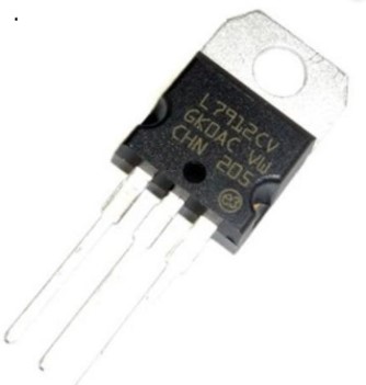
LM7912 IC – 12V Negative Voltage Regulator IC
The LM7912 series of three-terminal negative regulators are available in the TO-220 package and with several fixed output voltages, making them useful in a wide range of applications. Each type employs internal current limiting, thermal shut down, and safe operating area protection, making it essentially indestructible.
The LM337?is a Variable Negative Voltage Regulator that can output voltage from -1.25V to -37V with a maximum output current of -1.5A


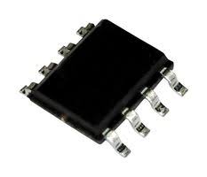
LM833 Dual Low Noise Audio Op-Amp IC DIP-8
The LM833 is a standard low?cost monolithic dual general?purpose operational amplifier employing Bipolar technology with innovative high?performance concepts for audio systems applications. With high frequency PNP transistors, the LM833 offers low voltage noise (4.5 nV/ Hz ), 15 MHz gain bandwidth product, 7.0 V/s slew rate, 0.3 mV input offset voltage with 2.0 V/?C temperature coefficient of input offset voltage. The LM833 output stage exhibits no dead?band crossover distortion, large output voltage swing, excellent phase and gain margins, low open loop high frequency output impedance and symmetrical source/sink AC frequency response.
LMC567CM
Functionally Similar to LM567
LMCMOS tone decoder which is functionally similar
? 2-V to 9-V Supply Voltage Range to the industry standard LM567. The device consists
? Low Supply Current Drain of a twice frequency voltage-controlled oscillator
? No Increase in Current With Output Activated (VCO) and quadrature dividers which establish the
reference signals for phase and amplitude detectors.
? Operates to 500-kHz Input Frequency
? High Oscillator Stability The phase detector and VCO form a phase-locked
loop (PLL) which locks to an input signal frequency
? Ground-Referenced Input which is within the control range of the VCO. When
? Hysteresis Added to Amplitude Comparator the PLL is locked and the input signal amplitude
? Out-of-Band Signals and Noise Rejected exceeds an internally pre-set threshold, a switch to
ground is activated on the output pin. External ? 20-mA Output Current Capability
LMC660AIN
Rail-to-Rail Output Swing
ideal for operation from a single supply. It operates
? Specified for 2 k? and 600? Loads from 5V to 15.5V and features rail-to-rail output
? High Voltage Gain: 126 dB swing in addition to an input common-mode range
that includes ground. Performance limitations that ? Low Input Offset Voltage: 3 mV
have plagued CMOS amplifiers in the past are not a
? Low Offset Voltage Drift: 1.3 ?V/?C
problem with this design. Input VOS, drift, and
? Ultra Low Input Bias Current: 2 fA broadband noise as well as voltage gain into realistic
? Input Common-Mode Range Includes V loads (2 k? and 600?) are all equal to or better than ?
widely accepted bipolar equivalents. ? Operating Range from 5V to 15.5V Supply
? I This chip is built with TI's advanced Double-Poly SS = 375 ?A/Amplifier; Independent of V
Silicon-Gate CMOS process.
? Low Distortion: 0.01% at 10 kHz
? Slew Rate: 1.1 V/?s

LMC660CN
The LMC660 CMOS Quad operational amplifier is ? Rail-to-Rail Output Swing
ideal for operation from a single supply. It operates
? Specified for 2 k? and 600? Loads from 5V to 15.5V and features rail-to-rail output
? High Voltage Gain: 126 dB swing in addition to an input common-mode range
that includes ground. Performance limitations that ? Low Input Offset Voltage: 3 mV
have plagued CMOS amplifiers in the past are not a
? Low Offset Voltage Drift: 1.3 ?V/?C
problem with this design. Input VOS, drift, and
? Ultra Low Input Bias Current: 2 fA broadband noise as well as voltage gain into realistic
? Input Common-Mode Range Includes V loads (2 k? and 600?) are all equal to or better than ?
widely accepted bipolar equivalents

LMC662CM
The LMC662 CMOS Dual operational amplifier is ? Rail-to-Rail Output Swing
ideal for operation from a single supply. It operates
? Specified for 2 k? and 600? Loads from 5V to 15V and features rail-to-rail output
? High Voltage Gain: 126 dB swing in addition to an input common-mode range
that includes ground. Performance limitations that ? Low Input Offset Voltage: 3 mV
have plagued CMOS amplifiers in the past are not a
? Low Offset Voltage Drift: 1.3 ?V/?C
problem with this design. Input VOS, drift, and
? Ultra Low Input Bias Current: 2 fA broadband noise as well as voltage gain into realistic
? Input Common-Mode Range Includes V loads (2 k? and 600?) are all equal to or better than ?
widely accepted bipolar equivalents. ? Operating Range from 5V to 15V Supply
? I This chip is built with TI's advanced Double-Poly SS = 400 ?A/amplifier; Independent of V
Silicon-Gate CMOS process.
? Low Distortion: 0.01% at 10 kHz
? Slew Rate: 1.1 V/?s See the LMC660 datasheet for a Quad CMOS
operational amplifier with these same features.

LNK302PN
LinkSwitch-TN is specifically designed to replace all linear and
capacitor-fed (cap dropper) non-isolated power supplies in the
under 360 mA output current range at equal system cost while
offering much higher performance and energy efficiency.
LinkSwitch-TN devices integrate a 700 V power MOSFET,
oscillator, simple On/Off control scheme, a high-voltage switched
current source, frequency jittering, cycle-by-cycle current limit

LNK304PN
Universal AC input range ? single design worldwide
Accurate and stable constant current output
Small size and weight
Low cost, low component count solution replaces passive
capacitor or resistor droppers
Fail safe topology ? protects load
High effi ciency (>60% at 85 VAC)
Scalable output power using larger LinkSwitch-TN devices
Meets EN55022 B EMI limits
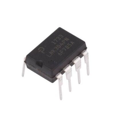
LNK304PN IC – Power Integrations – AC-DC Off Line Switcher IC
The LNK304PN is specifically designed to replace all linear and capacitor-fed (cap dropper) non-isolated power supplies in the under 360 mA output current range at equal system cost while offering much higher performance and energy efficiency. LinkSwitch-TN devices integrate a 700 V power MOSFET, oscillator, simple On/Off control scheme, a high-voltage switched current source, frequency jittering, cycle-by-cycle current limit Figure 1. Typical Buck Converter Application (See Application Examples Section ? ?for Other Circuit Configurations).and thermal shutdown circuitry onto a monolithic IC. The start-up and operating power are derived directly from the voltage on the DRAIN pin, eliminating the need for a bias supply and associated circuitry in buck or fly back converters. The fully integrated auto-restart circuit in the LNK304 safely limits output power during fault conditions such as short-circuit or open loop, reducing component count and system-level load protection cost. ?A local supply provided by the IC allows use of a non-safety graded optocoupler acting as a level shifter to further enhance line and load regulation performance in buck and buck-boost converters.


