


TPS22976DPUT
₹32.00
Features of TPS22976DPUT
? Dual-channel integrated load switch
? 0.6 to VBIAS for the input voltage range
? Voltage range for VBIAS: 2.5 to 5.7 V
? Maximum channel continuous switch current of 6 A
? Use of 1.2-, 1.8-, 2.5-, and 3.3-V logic is possible when the control input threshold is met.
? Easily adjustable rising time
? Short time to turn on
? Thermal braking
? QOD, or quick output discharge (optional)
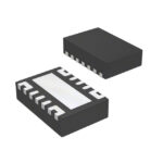
? Thermal pad on SON 14-pin box
? ESD performance assessed according to JESD 22
Applications of TPS22976DPUT
? Ultrabook?
? Notebooks and Netbooks
? Tablet PCs
? Set-top Boxes and Residential Gateways
? Telecom Systems
? Solid-State Drives (SSD)
2866 in stock
Description of TPS22976DPUT
Three devices make up the TPS22976 product family: the TPS22976, TPS22976A, and TPS22976N.
Each component is a controlled turn-on dual-channel load switch. A maximum continuous current of 6 A per channel and an input voltage range of 0.6 V to 5.7 V are supported by the device’s two N-channel MOSFETs.
An on and off input (ON1 and ON2) that can connect with low-voltage control signals independently controls each switch. When the junction temperature rises over the threshold, the TPS22976 is capable of thermal shutdown, which turns off the switch. As soon as the junction temperature returns to a safe range, the switch is activated once more.
The TPS22976 is offered in a compact, 3-mm 2-mm 14-SON package (DPU), which saves space and enables high power dissipation. The system is designed to function in the -40?C to 105?C free-air temperature range.


MAECENAS IACULIS
Vestibulum curae torquent diam diam commodo parturient penatibus nunc dui adipiscing convallis bulum parturient suspendisse parturient a.Parturient in parturient scelerisque nibh lectus quam a natoque adipiscing a vestibulum hendrerit et pharetra fames nunc natoque dui.
ADIPISCING CONVALLIS BULUM
- Vestibulum penatibus nunc dui adipiscing convallis bulum parturient suspendisse.
- Abitur parturient praesent lectus quam a natoque adipiscing a vestibulum hendre.
- Diam parturient dictumst parturient scelerisque nibh lectus.
Scelerisque adipiscing bibendum sem vestibulum et in a a a purus lectus faucibus lobortis tincidunt purus lectus nisl class eros.Condimentum a et ullamcorper dictumst mus et tristique elementum nam inceptos hac parturient scelerisque vestibulum amet elit ut volutpat.
Related products
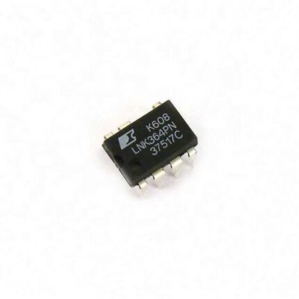
LNK364 IC – Low Power Offline Switcher IC

TNY267PN IC – Power Integrations Off Line Switcher IC
TNY268PN IC – Power Integrations Off Line Switcher with Low Power IC
TNY268PN IC - Low Power Off-Line Switcher - Power Integrations - DIP-8
The TNY268PN integrates a 700V power MOSFET, oscillator, high voltage switched current source, current limit, and thermal shutdown circuitry onto a monolithic device. The start-up and operating power are derived directly from the voltage on the DRAIN pin, eliminating the need for a bias winding and associated circuitry. In addition, the TNY268PN incorporates auto-restart, line under voltage sense, and frequency jittering. An innovative design minimizes audio frequency components in the simple ON/OFF control scheme to practically eliminate audible noise with standard taped/varnished transformer construction. The fully integrated auto-restart circuit safely limits output power during fault conditions such as output short circuits or open loop, reducing component count and secondary feedback circuitry cost.
TNY280PN IC – Power Integrations AC/DC Converter IC
TNY280PN IC - TinySwitch?-III energy-efficient, off-line switcher with enhanced flexibility and extended power range that incorporates a 700V power MOSFET, oscillator, high-voltage switched current source, current limit (user selectable), and thermal shutdown circuitry. The IC family uses an ON/OFF control scheme and offers a design flexible solution with a low system cost and extended power capability. The application includes chargers/adapters for cell/cordless phones, PDAs, digital cameras, MP3/portable audio, shavers, PC standby and other auxiliary supplies, DVD/PVR, and other low-power set-top decoders, supplies for appliances, industrial systems, and metering. ON/OFF control provides constant efficiency down to a very light load and it is ideal for mandatory CEC regulations and 1W PC standby requirements. Very low component count enhances reliability and enables a single-sided printed circuit board layout. High bandwidth provides fast turn-on with no overshoot and excellent transient load response.

TNY288PG IC – Power Integrations Off Line Switcher IC
- Lowest System Cost with Enhanced Flexibility
- 725 V rated MOSFET
- Increases BV de-rating margin
- Line compensated overload power ? no additional components
- Dramatically reduces max overload variation over universal input voltage range
- ?5% turn on UV threshold: line voltage sense with single external resistor
- Simple ON/OFF control, no loop compensation needed
- Selectable current limit through BP/M capacitor value
- Higher current limit extends peak power or, in open frame applications, maximum continuous power
- Lower current limit improves efficiency in enclosed adapters/ chargers
- Allows optimum TinySwitch?-4 choice by swapping devices with no other circuit redesign
- Tight I2 f parameter tolerance reduces system cost
- Maximizes MOSFET and magnetics utilization
- ON-time extension ? extends low-line regulation range/hold-up time to reduce input bulk capacitance
- Self-biased: no bias winding or bias components
- Frequency jittering reduces EMI filter costs
- Pin-out simplifies heat sinking to the PCB
- SOURCE pins are electrically quiet for low EMI

TOP227YN IC – Power Integrations – Off Line Switcher IC

TOP245YN IC – Power Integrations – Off Line Switcher IC


Reviews
There are no reviews yet.