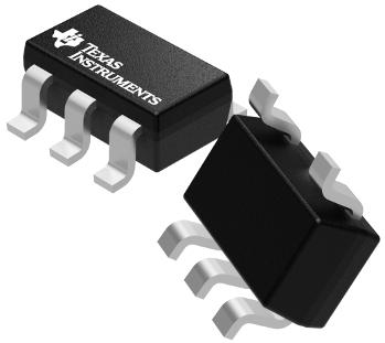
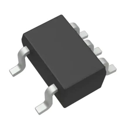
TPS2041BDBVR
₹47.00
Features of TPS2041BDBVR
- High-Side MOSFET of 70 m
- Continuous Current of 500 mA
- Protection against Thermal and Short Circuits
- Valid Current Limit (0.75 A Minimum, 1.25 A Maximum)
- Range of Operation: 2.7 to 5.5 V
- Typical Rise Time of 0.6 ms
- Overcurrent Lockout
- Report of a Deglitched Fault (OC)
- Power Up Has No OC Glitch
- 1-A (single, dual) or 2-A is the maximum standby supply current (Triple, Quad)
- -40?C to 85?C in the ambient temperature
- UL Approved, File No. E169910
- Additional UL Recognition for the Ganged Configuration TPS2042B and TPS2052B
Applications of TPS2041BDBVR
? Significant Capacitive Loads
? Short-Circuit Safety Measures
2880 in stock
Description of TPS2041BDBVR
The TPS2041BDBVR power-distribution switches are designed for use in settings where short circuits and large capacitive loads are common. For power-distribution systems that need several power switches in a single package, these devices integrate 70-m N-channel MOSFET power switches.
A logic enable input controls each switch. Gate drive is provided by an internal charge pump that regulates the rise and fall times of the power switch to reduce current surges during switching. The charge pump works with supply as low as 2.7 V and doesn’t need any other components.
The device restricts the output current to a safe level by switching into a constant-current mode and lowering the overcurrent (OCx) logic output when the output load exceeds the current-limit threshold or a short is present.
A thermal protection circuit turns off the switch to prevent damage when frequent heavy overloads and short circuits raise the power dissipation in the switch and cause the junction temperature to rise. Once the component has cooled down enough, recovery from a thermal shutdown happens automatically.
The switch’s internal circuitry makes sure it stays off until a valid input voltage is available. The current limit on this power distribution switch is set at 1 A. (typical).


MAECENAS IACULIS
Vestibulum curae torquent diam diam commodo parturient penatibus nunc dui adipiscing convallis bulum parturient suspendisse parturient a.Parturient in parturient scelerisque nibh lectus quam a natoque adipiscing a vestibulum hendrerit et pharetra fames nunc natoque dui.
ADIPISCING CONVALLIS BULUM
- Vestibulum penatibus nunc dui adipiscing convallis bulum parturient suspendisse.
- Abitur parturient praesent lectus quam a natoque adipiscing a vestibulum hendre.
- Diam parturient dictumst parturient scelerisque nibh lectus.
Scelerisque adipiscing bibendum sem vestibulum et in a a a purus lectus faucibus lobortis tincidunt purus lectus nisl class eros.Condimentum a et ullamcorper dictumst mus et tristique elementum nam inceptos hac parturient scelerisque vestibulum amet elit ut volutpat.










Reviews
There are no reviews yet.