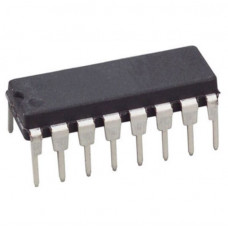
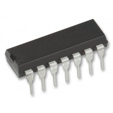
CD4099 8 bit Addressable Latch IC DIP-16 Package
₹21.00
CD4099 8-bit addressable latch is a serial-input, parallel-output storage register that can perform a variety of functions.
Data are inputted to a particular bit in the latch when that bit is addressed (by means of input A0, A1, A2) and when WRITE DISABLE is at a low level. When WRITE DISABLE is high, data entry is inhibited; however, all 8 outputs can be continuously read independent of WRITE DISABLE and address inputs.
A master RESET input is available, which resets all bits to a logic “0” level when RESET and WRITE DISABLE are at a high level. When RESET is at a high level, and WRITE RESET is at a low level, the latch acts as a 1-of-8 demultiplexer; the bit that is addressed has an active output which follows the data input, while all unaddressed bits are held to a logic “0” level.
The CD4099 types are supplied in 16-lead hermetic dual-in-line ceramic packages (F3A suffix), 16-lead dual-in-line plastic package (E suffix), 16-lead small-outline package (M, M96, MT, and NSR suffixes), and 16-lead thin shrink small-outline packages (PW and PWR suffixes).
Features:-
- Serial data input
- Active parallel output
- Storage register capability
- Master clear
- Can function as demultiplexer
- Standardized, symmetrical output characteristics
- 100% tested for quiescent current at 20 V
- Maximum input current of 1 uA at 18 V over full package-temperature range; 100 nA at 18 V and 25?C
- Noise margin (full package-temperature range) =
1 V at VDD?= 5 V
2 V at VDD?= 10 V
2.5 V at VDD?= 15 V - 5-V, 10-V, and 15-V parametric ratings
- Meets all requirements of JEDEC Tentative Standard No. 13B, “Standard Specifications for Description of ?B? Series CMOS Devices”
- Applications:
- Multi-line decoders
- A/D converters
Specifications:-
| Parameter | Specification |
| Part number | CD4099B |
| Technology Family | CD4000 |
| VCC (Min) (V) | 3 |
| VCC (Max) (V) | 18 |
| Bits (#) | 8 |
| Voltage (Nom) (V) | 10 |
| F @ nom voltage (Max) (MHz) | 8 |
| ICC @ nom voltage (Max) (mA) | 0.3 |
| tpd @ nom Voltage (Max) (ns) | 150 |
| IOL (Max) (mA) | 1.5 |
| IOH (Max) (mA) | -1.5 |
| 3-state output | No |
| Operating temperature range (C) | -55 to 125 |
Related Document:-
 ?CD4099 IC Datasheet
* Product Images are shown for illustrative purposes only and may differ from actual product.


MAECENAS IACULIS
Vestibulum curae torquent diam diam commodo parturient penatibus nunc dui adipiscing convallis bulum parturient suspendisse parturient a.Parturient in parturient scelerisque nibh lectus quam a natoque adipiscing a vestibulum hendrerit et pharetra fames nunc natoque dui.
ADIPISCING CONVALLIS BULUM
- Vestibulum penatibus nunc dui adipiscing convallis bulum parturient suspendisse.
- Abitur parturient praesent lectus quam a natoque adipiscing a vestibulum hendre.
- Diam parturient dictumst parturient scelerisque nibh lectus.
Scelerisque adipiscing bibendum sem vestibulum et in a a a purus lectus faucibus lobortis tincidunt purus lectus nisl class eros.Condimentum a et ullamcorper dictumst mus et tristique elementum nam inceptos hac parturient scelerisque vestibulum amet elit ut volutpat.


