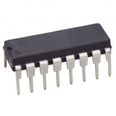

CD4066 Quad Bilateral Switch IC DIP-14 Package
₹15.00
The CD4066 device is a quad bilateral switch intended for the transmission or multiplexing of analog or digital signals. It is pin-for-pin compatible with the CD4016 device, but exhibits a much lower on-state resistance.
The CD4066 device consists of four bilateral switches, each with independent controls. Both the p and the n devices in a given switch are biased on or off simultaneously by the control signal. The well of the n-channel device on each switch is tied to either the input (when the switch is on) or to VSS?(when the switch is off). This configuration eliminates the variation of the switch-transistor threshold voltage with input signal and, thus, keeps the on-state resistance low over the full operating-signal range.
The advantages over single-channel switches include peak input-signal voltage swings equal to the full supply voltage and more constant on-state impedance over the input-signal range. However, for sample-and-hold applications, the CD4016 device is recommended.
Features:-
- 15-V Digital or ?7.5-V Peak-to-Peak Switching
- 125-? Typical On-State Resistance for
15-V Operation - Switch On-State Resistance Matched to Within
5 ? Over 15-V Signal-Input Range - On-State Resistance Flat Over Full
Peak-to-Peak Signal Range - High On or Off Output-Voltage Ratio:
80 dB Typical at fis?= 10 kHz, RL?= 1 k? - High Degree of Linearity: <0.5% Distortion Typical at fis?= 1 kHz, Vis?= 5-Vp-p
VDD?? VSS?? 10-V, RL?= 10 k? - Extremely Low Off-State Switch Leakage, Resulting in Very Low Offset Current and High Effective Off-State Resistance: 10 pA Typical at VDD?? VSS?= 10-V, TA?= 25?C
- Extremely High Control Input Impedance
(Control Circuit Isolated From Signal Circuit):
1012?? Typical - Low Crosstalk Between Switches: ?50 dB Typical at fis?= 8 MHz, RL?= 1 k?
- Matched Control-Input to Signal-Output Capacitance: Reduces Output Signal Transients
- Frequency Response,
Switch On = 40 MHz Typical - 100% Tested for Quiescent Current at 20-V
- 5-V, 10-V, and 15-V Parametric Ratings
?
Specifications:-
| Parameter | Specification |
| Part number | CD4066B |
| Configuration | 1:1 SPST |
| Number of channels (#) | 4 |
| Ron (Typ) (Ohms) | 125 |
| Bandwidth (MHz) | 40 |
| Rating | See Data Sheet |
| Operating temperature range (C) | -55 to 125 |
| Package Group | PDIP|14 |
| Input/output continuous current (Max) (mA) | 10 |
| Supply current (Typ) (uA) | 0.01 |
| CON (Typ) (pF) | 8 |
Related Document:-
 ?CD4066 IC Datasheet
* Product Images are shown for illustrative purposes only and may differ from actual product.


MAECENAS IACULIS
Vestibulum curae torquent diam diam commodo parturient penatibus nunc dui adipiscing convallis bulum parturient suspendisse parturient a.Parturient in parturient scelerisque nibh lectus quam a natoque adipiscing a vestibulum hendrerit et pharetra fames nunc natoque dui.
ADIPISCING CONVALLIS BULUM
- Vestibulum penatibus nunc dui adipiscing convallis bulum parturient suspendisse.
- Abitur parturient praesent lectus quam a natoque adipiscing a vestibulum hendre.
- Diam parturient dictumst parturient scelerisque nibh lectus.
Scelerisque adipiscing bibendum sem vestibulum et in a a a purus lectus faucibus lobortis tincidunt purus lectus nisl class eros.Condimentum a et ullamcorper dictumst mus et tristique elementum nam inceptos hac parturient scelerisque vestibulum amet elit ut volutpat.