

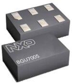


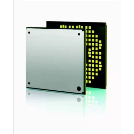
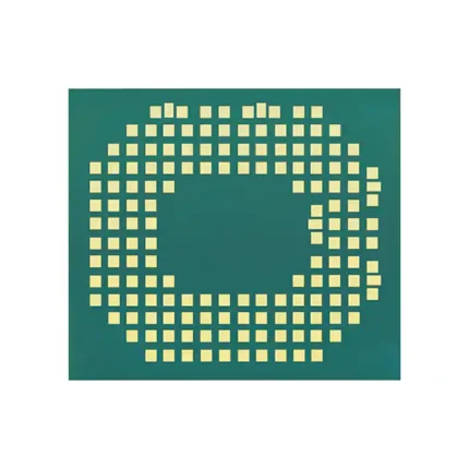
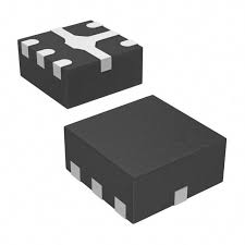
BGU7005
₹23.00
Benefits and features of BGU7005
- Covers the entire GNSS L1 range, 1559 to 1610 MHz
- Noise figure (NF) is equal to 0.85 dB.
- Increase 16.5 dB
- A lot of input Pi(1dB), or 1 dB compression point, is 11 dBm.
- High IP3i out of band of 9 dBm
- 1.5 to 3.1 volts is the supply voltage.
- Consumption of current in power-saving mode is 1 A.
- Optimized performance at 4.5 mA, a low supply current
- Output matching that is integrated
- Only needs one supply decoupling capacitor and one input matching inductor.
- Decoupled DC input and output
- All pins have ESD protection (HBM > 2 kV).
- Temperature-stabilized bias included for simple design
- Small leadless 6-pin package 1.45 mm, 1 mm, and 0.5 mm
- Transit frequency of 110 GHz using SiGe:C technology
2000 in stock
Description of BGU7005?
The BGU7005 is a Low Noise Amplifier (LNA) for GNSS receiver applications in a plastic leadless 6-pin, incredibly compact SOT886 packaging, commonly known as the GPS1101M. Only one external matching inductor and one external decoupling capacitor are needed for the BGU7005.
The BGU7005 adapts to the shifting environment brought on by the coexistence of many radio systems in contemporary cell phones. When coexisting cellular transmitters are available, it has been engineered to consume less power and operate at its best.
It provides 16.5 dB gain at a noise figure of 0.85 dB at low jamming power levels. It briefly boosts its bias current to increase sensitivity when there are high jamming power levels, such as during a cellular transmit burst.


MAECENAS IACULIS
Vestibulum curae torquent diam diam commodo parturient penatibus nunc dui adipiscing convallis bulum parturient suspendisse parturient a.Parturient in parturient scelerisque nibh lectus quam a natoque adipiscing a vestibulum hendrerit et pharetra fames nunc natoque dui.
ADIPISCING CONVALLIS BULUM
- Vestibulum penatibus nunc dui adipiscing convallis bulum parturient suspendisse.
- Abitur parturient praesent lectus quam a natoque adipiscing a vestibulum hendre.
- Diam parturient dictumst parturient scelerisque nibh lectus.
Scelerisque adipiscing bibendum sem vestibulum et in a a a purus lectus faucibus lobortis tincidunt purus lectus nisl class eros.Condimentum a et ullamcorper dictumst mus et tristique elementum nam inceptos hac parturient scelerisque vestibulum amet elit ut volutpat.
Related products


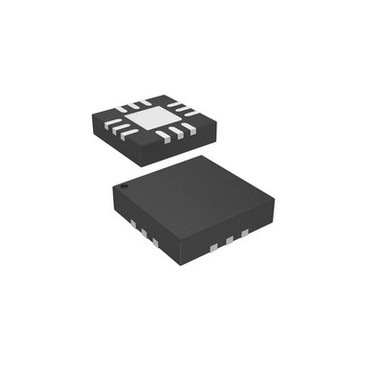
CC2592RGV
- LNA Gain Digitally Controlled via an HGM Terminal
- (LNA EN = PA EN = 0) 100 nA in Power Down
- Little Transmit Current Use -PAE = 34% at -155 mA at 3 V for +22 dBm
- Low Receiving Current Intake -For High-Gain Mode, use -4.0 mA -For Low-Gain Mode, -1.9 mA
- T/R Switch and External Antenna Match Included in the 4.7-dB LNA Noise Figure
- Conforms to RoHS QFN-16 Package, 4-mm by 4-mm
- Operation from 2.0-V to 3.7-V
- Operating Range: -40?C to +125?C
- Texas Instruments' Seamless Interface to 2.4-GHz Low-Power RF Devices
- Power Output: +22 dBm
- Improved Sensitivity of 3 dB Typically on CC2520, CC253X, and CC85XX
- Almost No External Components -Switches that are built-in -Network for Integrated Matching -Balun integrated -Integral Inductors -Integration of PA -LNA integrated
- Every 2.4-GHz ISM Band Device
- Gateways for ZigBee and IEEE 802.15.4
- Sensor Networks, Wireless
- Consumer Wireless Systems
- Industrial Wireless Systems
- Systems for Wireless Audio
- Metering systems utilizing IEEE 802.15.4 and ZigBee?

HT12D Decoder IC

L30960-N3400-A400
- LTE (20,8,3,7,1); 3G (8,3); and 2G Dual Band PLS8-E
- PLS8-US: 3G (5,4,2), 2G Quad Band, and LTE (17,5,4,2).
- LTE (1,3,19); 3G; PLS8-J (1,19)
- PLS8-X: 3G (5,4,2), 2G Quad Band, and LTE (13,17,5,4,2).
- LTE PLS8-V: (13,4,2)
- LTE (2x2 DL-MIMO; FDD 3GPP Release 9)
- 3GPP Release 8; UMTS/HSPA (FDD); Rx diversity
- 3GPP Release 6; DARP/SAIC; GSM/GPRS/EDGE
- SIM Application Toolkit, version 99 of the 3GPP
- Using AT instructions to control (Hayes, TS 27.007, TS 27.005)
- Complete GPS/GLONASS integration (Qualcomm gpsOne Gen8A)
- 3.3 to 4.2 V supply voltage range, especially tuned for low power usage
- Dimensions are 29 mm by 33 mm by 2,2 mm (PLS8-V/-X: H=2,9 mm).
- Range of Operation: -40 ?C to +85 ?C
- EuP support, RoHS and REACH compliance
- Multiple composite modes and a Linux/Mac-compliant mode are supported by the USB interface.
- USB-based firmware update
- BIP (Bearer Independent Protocol) (Bearer Independent Protocol)
- From Rel.3.0 and for PLS8-X /-V, IP services (Client & Server, TCP/IP & UDP, Transparent & Nontransparent) are available.
- According to 3GPP TS 27.010, a multiplexer
- Carrier Switching Automatic (PLS8-X)
L30960-N3410-A400
- LTE (20,8,3,7,1); 3G (8,3); and 2G Dual Band PLS8-E
- PLS8-US: 3G (5,4,2), 2G Quad Band, and LTE (17,5,4,2).
- LTE (1,3,19); 3G; PLS8-J (1,19)
- PLS8-X: 3G (5,4,2), 2G Quad Band, and LTE (13,17,5,4,2).
- LTE PLS8-V: (13,4,2)
- LTE (2x2 DL-MIMO; FDD 3GPP Release 9)
- 3GPP Release 8; UMTS/HSPA (FDD); Rx diversity
- 3GPP Release 6; DARP/SAIC; GSM/GPRS/EDGE
- SIM Application Toolkit, version 99 of the 3GPP
- Using AT instructions to control (Hayes, TS 27.007, TS 27.005)
- Complete GPS/GLONASS integration (Qualcomm gpsOne Gen8A)
- 3.3 to 4.2 V supply voltage range, especially tuned for low power usage
- Dimensions are 29 mm by 33 mm by 2,2 mm (PLS8-V/-X: H=2,9 mm).
- Range of Operation: -40 ?C to +85 ?C
- EuP support, RoHS and REACH compliance
- Multiple composite modes and a Linux/Mac-compliant mode are supported by the USB interface.
- USB-based firmware update
- BIP (Bearer Independent Protocol) (Bearer Independent Protocol)
- From Rel.3.0 and for PLS8-X /-V, IP services (Client & Server, TCP/IP & UDP, Transparent & Nontransparent) are available.
- According to 3GPP TS 27.010, a multiplexer
- PLS8-X Automatic Carrier Switching

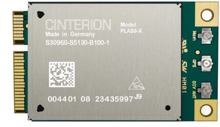
L30960-N5130-B100
- LTE (2x2 DL-MIMO; FDD 3GPP Release 9)
- 3GPP Release 8; UMTS/HSPA (FDD); Rx diversity
- 3GPP Release 6; DARP/SAIC; GSM/GPRS/EDGE
- SIM Application Toolkit, version 99 of the 3GPP
- Using AT instructions to control (Hayes, TS 27.007, TS 27.005)
- 3.3 to 4.2 V supply voltage range, especially tuned for low power usage
- Size: 40, 32, and 2,8 mm
- Range of Operation Temperature: -40 ?C to +95 ?
- Compliant with RoHS, RED, and REACH, EuP assistance
- The USB 2.0/3.0 interface provides several composite modes and a mode that is compatible with Linux and Mac.
- USB-based firmware update
SKY13323-378LF
- Control of positive voltage (0 and 1.8 V to 0 and 5.0 V)
- The frequency range for broadband is 0.1-3.0 GHz.
- Very low insertion loss, typically 0.35 dB at 3 GHz
- High isolation, typical 27 dB @ 3 GHz
- P1dB = +27 dBm, excellent linearity performance
- MLPD (6-pin, 1 x 1 mm, MSL1, 260 ?C per JEDEC J-STD-020) ultra-compact packaging
- 802.11 b/g WLAN networks
- Wi-Fi repeaters
- ISM-band radios
- Systems for low-power transmission and reception

SKY13374-397LF
- The frequency range for broadband is 300 kHz to 6.0 GHz.
- Low insertion loss at 1 GHz and 6 GHz: 0.35 dB and 0.8 dB, respectively
- There is no need for external DC blocking capacitors.
- 1.65 to 3.0 V (VCTRL), 2.5 to 4.8 V are examples of positive low control voltages (VBATT)
- QFN (12-pin, 2 x 2 mm) small packaging (MSL1, 260 C per JEDEC J-STD-020)
- Wireless LANs with dual bands (802.11 a/b/g/n)
- Switching between diversity antennas
- WCDMA mobile phones and data cards
- SPDT switch configuration
- Frequency Minimum: 300 kHz
- 6 GHz maximum frequency
- Loss of Insertion: 0.8 dB
- Type of Off Isolation: 2 dB
- 40 C for the minimum operating temperature
- 85 C is the maximum operating temperature.
- SMD/SMT mounting style
- Technology: Si
- Packaging: Reel/ Cut Tape


Reviews
There are no reviews yet.