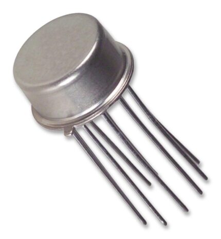


LMC567CM
Functionally Similar to LM567
LMCMOS tone decoder which is functionally similar
? 2-V to 9-V Supply Voltage Range to the industry standard LM567. The device consists
? Low Supply Current Drain of a twice frequency voltage-controlled oscillator
? No Increase in Current With Output Activated (VCO) and quadrature dividers which establish the
reference signals for phase and amplitude detectors.
? Operates to 500-kHz Input Frequency
? High Oscillator Stability The phase detector and VCO form a phase-locked
loop (PLL) which locks to an input signal frequency
? Ground-Referenced Input which is within the control range of the VCO. When
? Hysteresis Added to Amplitude Comparator the PLL is locked and the input signal amplitude
? Out-of-Band Signals and Noise Rejected exceeds an internally pre-set threshold, a switch to
ground is activated on the output pin. External ? 20-mA Output Current Capability
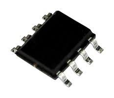
LMC660AIN
Rail-to-Rail Output Swing
ideal for operation from a single supply. It operates
? Specified for 2 k? and 600? Loads from 5V to 15.5V and features rail-to-rail output
? High Voltage Gain: 126 dB swing in addition to an input common-mode range
that includes ground. Performance limitations that ? Low Input Offset Voltage: 3 mV
have plagued CMOS amplifiers in the past are not a
? Low Offset Voltage Drift: 1.3 ?V/?C
problem with this design. Input VOS, drift, and
? Ultra Low Input Bias Current: 2 fA broadband noise as well as voltage gain into realistic
? Input Common-Mode Range Includes V loads (2 k? and 600?) are all equal to or better than ?
widely accepted bipolar equivalents. ? Operating Range from 5V to 15.5V Supply
? I This chip is built with TI's advanced Double-Poly SS = 375 ?A/Amplifier; Independent of V
Silicon-Gate CMOS process.
? Low Distortion: 0.01% at 10 kHz
? Slew Rate: 1.1 V/?s

LMC660CN
The LMC660 CMOS Quad operational amplifier is ? Rail-to-Rail Output Swing
ideal for operation from a single supply. It operates
? Specified for 2 k? and 600? Loads from 5V to 15.5V and features rail-to-rail output
? High Voltage Gain: 126 dB swing in addition to an input common-mode range
that includes ground. Performance limitations that ? Low Input Offset Voltage: 3 mV
have plagued CMOS amplifiers in the past are not a
? Low Offset Voltage Drift: 1.3 ?V/?C
problem with this design. Input VOS, drift, and
? Ultra Low Input Bias Current: 2 fA broadband noise as well as voltage gain into realistic
? Input Common-Mode Range Includes V loads (2 k? and 600?) are all equal to or better than ?
widely accepted bipolar equivalents

LMC662CM
The LMC662 CMOS Dual operational amplifier is ? Rail-to-Rail Output Swing
ideal for operation from a single supply. It operates
? Specified for 2 k? and 600? Loads from 5V to 15V and features rail-to-rail output
? High Voltage Gain: 126 dB swing in addition to an input common-mode range
that includes ground. Performance limitations that ? Low Input Offset Voltage: 3 mV
have plagued CMOS amplifiers in the past are not a
? Low Offset Voltage Drift: 1.3 ?V/?C
problem with this design. Input VOS, drift, and
? Ultra Low Input Bias Current: 2 fA broadband noise as well as voltage gain into realistic
? Input Common-Mode Range Includes V loads (2 k? and 600?) are all equal to or better than ?
widely accepted bipolar equivalents. ? Operating Range from 5V to 15V Supply
? I This chip is built with TI's advanced Double-Poly SS = 400 ?A/amplifier; Independent of V
Silicon-Gate CMOS process.
? Low Distortion: 0.01% at 10 kHz
? Slew Rate: 1.1 V/?s See the LMC660 datasheet for a Quad CMOS
operational amplifier with these same features.


LT1004IS8-1.2
The micropower voltage reference is a
2-terminal bandgap reference diode designed to provide
high accuracy and excellent temperature characteristics
at very low operating currents. Optimization of the key
parameters in the design, processing and testing of
the device results in accuracy specifications previously
attainable only with selected units. Below is a distribution
plot of reference voltage for a typical lot of LT1004-1.2.
Virtually all of the units fall well within the prescribed
limits of ?4mV.
The LT1004 is a pin-for-pin replacement for the
LM185/LM385 series of references with improved accuracy specifications. More important, the LT1004 is an
attractive device for use in systems where accuracy was
previously obtained at the expense of power consumption and trimming.

LT1009CZ
The LT?1009 is a precision trimmed 2.5V shunt regulator diode featuring a maximum initial tolerance of only
?5mV. The low dynamic impedance and wide operating
current range enhances its versatility. The 0.2% reference
tolerance is achieved by on-chip trimming which not only
minimizes the initial voltage tolerance but also minimizes
the temperature drift.
Even though no adjustments are needed with the LT1009,
a third terminal allows the reference voltage to be adjusted
?5% to calibrate out system errors. In many applications,
the LT1009 can be used as a pin-to-pin replacement of the
LM136 and the external trim network eliminated.


