L6201
The I.C. is a full bridge driver for motor control applications realized in Multipower-BCD technology
which combines isolated DMOS power transistors
with CMOS and Bipolar circuits on the same chip.
By using mixed technology it has been possible to
optimize the logic circuitry and the power stage to
achieve the best possible performance. The
DMOS output transistors can operate at supply
voltages up to 42V and efficiently at high switching speeds. All the logic inputs are TTL, CMOS
and ?C compatible. Each channel (half-bridge) of
the device is controlled by a separate logic input,
while a common enable controls both channels.
The I.C. is mounted in three different packages.

L6203
The I.C. is a full bridge driver for motor control applications realized in Multipower-BCD technology
which combines isolated DMOS power transistors
with CMOS and Bipolar circuits on the same chip.
By using mixed technology it has been possible to
optimize the logic circuitry and the power stage to
achieve the best possible performance. The
DMOS output transistors can operate at supply
voltages up to 42V and efficiently at high switching speeds. All the logic inputs are TTL, CMOS
and ?C compatible. Each channel (half-bridge) of
the device is controlled by a separate logic input,
while a common enable controls both channels.
The I.C. is mounted in three different packages.
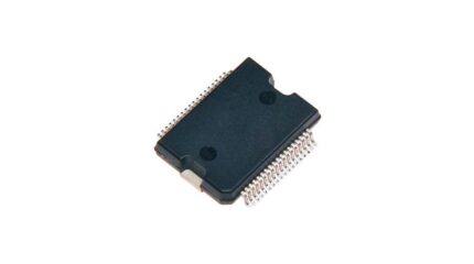
L6207PD
The L6207 device is a DMOS dual full bridge
designed for motor control applications, realized
in BCD technology, which combines isolated
DMOS power transistors with CMOS and bipolar
circuits on the same chip. The device also
includes two independent constant off time PWM
current controllers that perform the chopping
regulation. Available in PowerSO36 and SO24
(20 2 2) packages, the L6207 device features
a non-dissipative overcurrent protection on the
high-side Power MOSFETs and thermal
shutdown.

L6384D
The L6384 is a high-voltage device that utilizes BCD's "OFF-LINE" technology. It is equipped with a Half-Bridge Driver structure that allows it to drive N Channel Power MOS or IGBTs. The upper (floating) section can handle voltage rails up to 600V. For simplicity of connecting with controlling devices, the Logic Inputs are CMOS/TTL compatible. High-frequency functioning is made easier by matched delays between the Lower and Up-per Sections. With the help of an external resistor, you may easily set the dead time.
Features
HIGH VOLTAGE RAIL UP TO 600 V
dV/dt IMMUNITY - 50 V/n sec IN FULL TEMPERATURE RANGE
DRIVER CURRENT CAPABILITY: 400 mA SOURCE,650 mA SINK
SWITCHING TIMES 50/30 nsec RISE/FALLWITH 1nF LOAD
CMOS/TTL SCHMITT TRIGGER INPUT SWITH HYSTERESIS AND PULL DOWN
SHUT DOWN INPUT
DEAD TIME SETTING
UNDER VOLTAGE LOCK OUT
INTEGRATED BOOTSTRAP DIODE
CLAMPING ON Vcc
SO8/MINIDIP PACKAGES

L7812ABV
The L78 series of three-terminal positive regulators is available in TO-220,
TO-220FP, D?PAK and DPAK packages and several fixed output voltages, making it
useful in a wide range of applications.
These regulators can provide local on-card regulation, eliminating the distribution
problems associated with single point regulation. Each type embeds internal current
limiting, thermal shut-down and safe area protection, making it essentially
indestructible. If adequate heat sinking is provided, they can deliver over 1 A output
current. Although designed primarily as fixed voltage regulators, these devices can
be used with external components to obtain adjustable voltage and currents.

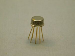
LF156H/883Q
The LFx5x devices are the first monolithic JFET input
Monolithic Amplifiers operational amplifiers to incorporate well-matched,
? New Output Stage Allows Use of Large high-voltage JFETs on the same chip with standard
Capacitive Loads (5,000 pF) Without Stability bipolar transistors (BI-FET? Technology). These
Problems amplifiers feature low input bias and offset
currents/low offset voltage and offset voltage drift,
? Internal Compensation and Large Differential coupled with offset adjust, which does not degrade Input Voltage Capability drift or common-mode rejection. The devices are also
? Common Features designed for high slew rate, wide bandwidth,
? Low extremely fast settling time, low voltage and current Input Bias Current: 30 pA
noise and a low 1/f noise corner
LF353H
This LF353 device is a low-cost, high-speed, JFETinput operational amplifier with very low input offset
voltage. It requires low supply current yet maintains a
large gain-bandwidth product and a fast slew rate. In
addition, the matched high-voltage JFET input
provides very low input bias and offset currents.
The LF353 can be used in applications such as highspeed integrators, digital-to-analog converters,
sample-and-hold circuits, and many other circuits.
The LF353 is characterized for operation from 0?C to
70?C.

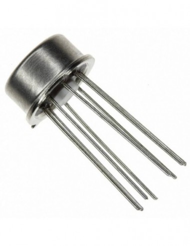

LF356H
The LF356-MIL device are the first monolithic JFET
input operational amplifiers to incorporate wellmatched, high-voltage JFETs on the same chip with
standard bipolar transistors (BI-FET? Technology).
These amplifiers feature low input bias and offset
currents/low offset voltage and offset voltage drift,
coupled with offset adjust, which does not degrade
drift or common-mode rejection. The devices are also
designed for high slew rate, wide bandwidth,
extremely fast settling time, low voltage and current
noise and a low 1/f noise corner.
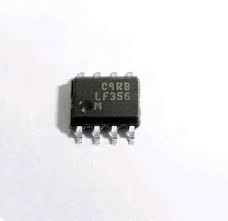
LF356M
The LFx5x devices are the first monolithic JFET input
Monolithic Amplifiers operational amplifiers to incorporate well-matched,
? New Output Stage Allows Use of Large high-voltage JFETs on the same chip with standard
Capacitive Loads (5,000 pF) Without Stability bipolar transistors (BI-FET? Technology). These
Problems amplifiers feature low input bias and offset
currents/low offset voltage and offset voltage drift,
? Internal Compensation and Large Differential coupled with offset adjust, which does not degrade Input Voltage Capability drift or common-mode rejection. The devices are also
? Common Features designed for high slew rate, wide bandwidth,
? Low extremely fast settling time, low voltage and current Input Bias Current: 30 pA
noise and a low 1/f noise corne


