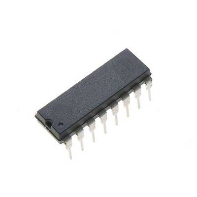
CD74ACT164E
The ?AC164 and ?ACT164 are 8-bit serial-in/parallel-out shift
registers with asynchronous reset that utilize Advanced
CMOS Logic technology. Data is shifted on the positive edge
of the clock (CP). A LOW on the Master Reset (MR) pin
resets the shift register and all outputs go to the LOW state
regardless of the input conditions. Two Serial Data inputs
(DS1 and DS2) are provided; either one can be used as a
Data Enable control.
CD74HC00M
This device contains four independent 2-input NAND
gates. Each gate performs the Boolean function
Y = A ? B in positive logic
1 Features
? Buffered inputs
? Wide operating voltage range: 2 V to 6 V
? Wide operating temperature range:
?55?C to 125?C
? Supports fanout up to 10 LSTTL loads
? Significant power reduction compared to LSTTL
logic ICs
CD74HC21E
This device contains two independent 4-input AND
gates. Each gate performs the Boolean function
Y = A ? B ? C ? D in positive logic
Buffered inputs
? Wide operating voltage range: 2 V to 6 V
? Wide operating temperature range:
-55?C to 125?C
? Supports fanout up to 10 LSTTL loads
? Significant power reduction compared to LSTTL
logic ICs
CD74HC40105E
This device contains two independent 4-input AND
gates. Each gate performs the Boolean function
Y = A ? B ? C ? D in positive logic.
Buffered inputs
? Wide operating voltage range: 2 V to 6 V
? Wide operating temperature range:
-55?C to 125?C
? Supports fanout up to 10 LSTTL loads
? Significant power reduction compared to LSTTL
logic IC
CD74HC4017E
The ?HC4017 is a high speed silicon gate CMOS 5-stage
Johnson counter with 10 decoded outputs. Each of the
decoded outputs is normally low and sequentially goes high
on the low to high transition clock period of the 10 clock
period cycle. The CARRY (TC) output transitions low to high
after OUTPUT 10 goes from high to low, and can be used in
conjunction with the CLOCK ENABLE (CE) to cascade
several stages. The CLOCK ENABLE input disables
counting when in the high state. A RESET (MR) input is also
provided which when taken high sets all the decoded
outputs, except ?0?, low.
The device can drive up to 10 low power Schottky equivalent
loads.
CD74HC540E
The ?HC540 and CD74HCT540 are Inverting Octal
Buffers and Line Drivers with Three-State Outputs
and the capability to drive 15 LSTTL loads.
The ?HC541 and ?HCT541 are Noninverting Octal
Buffers and Line Drivers with Three-State Outputs
that can drive 15 LSTTL loads. The Output Enables
(OE1) and (OE2) control the Three-State Outputs. If
either OE1 or OE2 is HIGH the outputs will be in the
high impedance state. For data output OE1 and OE2
both must be LOW.
CD74HC564E
The ?HC534, ?HCT534, ?HC564, and ?HCT564 are
high speed Octal D-Type Flip-Flops manufactured
with silicon gate CMOS technology. They possess the
low power consumption of standard CMOS integrated
circuits, as well as the ability to drive 15 LSTTL loads.
Due to the large output drive capability and the threestate feature, these devices are ideally suited for
interfacing with bus lines in a bus organized system.
The two types are functionally identical and differ only
in their pinout arrangements
CD74HCT08E
? LSTTL input logic compatible
? VIL(max) = 0.8 V, VIH(min) = 2 V
? CMOS input logic compatible
? II
? 1 ?A at VOL, VOH
? Buffered inputs
? 4.5 V to 5.5 V operation
? Wide operating temperature range:
-55?C to 125?C
? Supports fanout up to 10 LSTTL loads
? Significant power reduction compared to LSTTL
logic ICs


