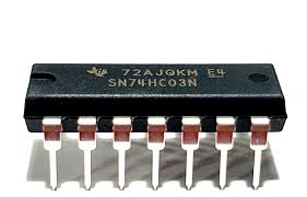
SN74HC03N
SN74HC08D
SN74HC164N
These 8-bit shift registers feature AND-gated serial
1? Wide Operating Voltage Range of 2 V to 6 V
inputs and an asynchronous clear (CLR) input. The
? Outputs Can Drive Up to 10 LSTTL Loads gated serial (A and B) inputs permit complete control
? Low Power Consumption, 80-?A Maximum ICC over incoming data; a low at either input inhibits entry
? Typical tpd = 20 ns of the new data and resets the first flip-flop to the low
level at the next clock (CLK) pulse. A high-level input
? ?4-mA Output Drive at 5 V
enables the other input, which then determines the
? Low Input Current of 1-?A Maximum state of the first flip-flop. Data at the serial inputs can
? AND-Gated (Enable/Disable) Serial Inputs be changed while CLK is high or low, provided the
minimum set-up time requirements are met. Clocking ? Fully Buffered Clock and Serial Inputs
occurs on the low-to-high-level transition of CLK.
SN74HC20N
SN74HC259N
These 8-bit addressable latches are designed for
general-purpose storage applications in digital
systems. Specific uses include working registers,
serial-holding registers, and active-high decoders
or demultiplexers. They are multifunctional
devices capable of storing single-line data in eight
addressable latches and being a 1-of-8 decoder
or demultiplexer with active-high outputs
SN74HC640N
These octal bus transceivers are designed for asynchronous two-way communication between data buses.
These devices transmit data from the A bus to the B bus or from the B bus to the A bus, depending upon the
level at the direction-control (DIR) input. The output-enable (OE) input can be used to disable the device so the
buses are effectively isolated
SN74HCT244DW
? Operating Voltage Range of 4.5 V to 5.5 V
? High-Current Outputs Drive up to 15 LSTTL Loads
? Low Power Consumption: 80-?A Maximum ICC
? Typical tpd = 13 ns
? ?6-mA Output Drive at 5 V
? Low Input Current of 1 ?A Maximum
? Inputs Are TTL-Voltage Compatible
? 3-State Outputs Drive Bus Lines and Buffer
Memory Address Registers
SN74HCT244PWG4
These octal buffers and line drivers are designed
specifically to improve both the performance and
density of 3-state memory address drivers,
clockdrivers, and bus-oriented receivers and
transmitters. The SNx4HCT244 devices are
organized as two 4-bit buffers or drivers with separate
output-enable (OE) inputs. When OE is low, the
device passes noninverted data from the A inputs to
the Y outputs. When OE is high, the outputs are in
the high-impedance state
SN74HCT540N
These octal buffers and line drivers are designed to have the performance of the ?HCT240 devices and a pinout
with inputs and outputs on opposite sides of the package. This arrangement greatly facilitates printed circuit
board layout.
The 3-state control gate is a 2-input NOR. If either output-enable (OE1 or OE2) input is high, all eight outputs
are in the high-impedance state. The ?HCT540 devices provide inverted data at the outputs.
To ensure the high-impedance state during power up or power down, OE should be tied to VCC through a pullup
resistor; the minimum value of the resistor is determined by the current-sinking capability of the
SN74LS00NS
? Package Options Include:
? Plastic Small-Outline (D, NS, PS)
? Shrink Small-Outline (DB)
? Ceramic Flat (W)
? Ceramic Chip Carriers (FK)
? Standard Plastic (N)
? Ceramic (J)
? Also Available as Dual 2-Input Positive-NAND
Gate in Small-Outline (PS) Package
? Inputs Are TTL Compliant; VIH = 2 V and
VIL = 0.8 V
? Inputs Can Accept 3.3-V or 2.5-V Logic Inputs
? SN5400, SN54LS00, and SN54S00 are
Characterized For Operation Over the Full Military
Temperature Range of ?55?C to 125?C


