Showing 181–192 of 734 results

ADS1230IPWR – 20 Bit Analog to Digital Converter For Bridge Sensors

180.00

ADS1230IPWR - 20-Bit, 80SPS, 1-Ch Delta-Sigma ADC for Resistive Bridge Sensors & Weigh Scales

The ADS1230 is a 20-bit precision analog-to-digital converter (ADC). The ADS1230 provides a full front-end system for bridge application areas such as weigh scales, strain gauges, and pressure sensors thanks to an inbuilt low-noise programmable gain amplifier (PGA), onboard oscillator, and precision 20-bit delta-sigma ADC. The low-noise PGA has a gain of 64 or 128, allowing for a full-scale differential input of 39mV or 19.5mV. The delta-sigma ADC has an effective resolution of 20 bits and is made up of a 3rd order modulator and a 4th order digital filter. APPLICATIONS
  • Weigh Scales
  • Strain Gauges
  • Pressure Sensors
  • Industrial Process Control

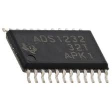
ADS1232IPWR -24-Bit, Delta-Sigma ADCs for Bridge Sensors

650.00

ADS1232IPWR is 24-bit precision analog-to-digital converter (ADCs). The ADS123x provides a full front-end solution for bridge sensor applications such as weigh scales, strain gauges, and pressure sensors thanks to its low-noise programmable gain amplifier (PGA), precision delta-sigma ADC, and internal oscillator. A differential input multiplexer (MUX) can receive two (ADS1232) or four (ADS1234) differential inputs. The ADS1232 also has a temperature sensor to monitor the outside temperature. The low-noise PGA supports a full scale differential input of 2.5 V, 1.25 V, 39 mV, or 19.5 mV and has a selectable gain of 1, 2, 64, or 128. The delta-sigma ADC has a maximum effective resolution of 23.5 bits and two data rates: 10 SPS (with 50-Hz and 60-Hz rejection) and 80 SPS.? directly connected to the MSP430 and other microcontrollers.

AM26C31 Differential Line Receiver (SOIC)

61.72

The AM26C31 is an improved replacement for?AM26LS31 IC.?The AM26C31 device is a quadruple differential line receiver for balanced or unbalanced digital data transmission. The enable function is common to all four receivers and offers a choice of active-high or active-low input. The 3-state outputs permit connection directly to a busorganized system. Fail-safe design specifies that if the inputs are open, the outputs always are high. The AM26C31 devices are manufactured using a BiCMOS process, which is a combination of bipolar and CMOS transistors

AM26C32 Differential Line Receiver (SOIC)

61.72

AM26C32 is an improved replacement for?AM26LS32 IC. The AM26C32 device is a quadruple differential line receiver for balanced or unbalanced digital data transmission. The enable function is common to all four receivers and offers a choice of active-high or active-low input. The 3-state outputs permit connection directly to a busorganized system. Fail-safe design specifies that if the inputs are open, the outputs always are high. The AM26C32 devices are manufactured using a BiCMOS process, which is a combination of bipolar and CMOS transistors.

AMS1117-3.3

10.00
The adjustable and fixed voltage regulators of the AMS1117 series are designed to deliver 1A output current and function down to 1V input-to-output difference. The device's dropout voltage is guaranteed to be 1.3V at maximum output current, dropping at lower load currents. Trimming on-chip adjusts the reference voltage to one percent. The current limit is also reduced, reducing stress on the regulator and energy source circuitry under overload conditions. The AMS1117 devices are pin compatible with existing three-terminal SCSI regulators and are available in low-profile surface mount SOT-223 packages, 8L SOIC packages, and TO-252 (DPAK) plastic packages.

AP7165-SPG-13

38.00
Features of AP7165-SPG-13 ? 2.2V to 5.5V, a broad input voltage range ? 500mA load with a 300mV very low dropout ? Extremely low quiescent current (IQ): typically 125 A ? Total accuracy is less than 2.5% for line, load, and temperature ? 0.8V to 5.0V adjustable output voltage range ? Extremely quick transient reaction ? A high PSRR. ? Reliable voltage control ? Current restriction and short circuit defence ? Thermal shut-off safeguards ? Stable with output capacitors of any kind up to 4.7 F ? A temperature range of -40 to +85 degrees Celsius. ? "Green" molding compound is available in U-DFN3030-10 and SO-8EP (No Br, Sb) ? RoHS Compliant and Lead Free Finish   Application of AP7165-SPG-13
  • Servers and laptops
  • Smart phone and PDA
  • MP3/MP4
  • Bluetooth headset
  • Low and medium power applications
  • FPGA and DSP core or I/O power

AT24C512-10PU

125.00
The AT24C512 provides 524,288 bits of serial electrically erasable and programmable read only memory (EEPROM) organized as 65,536 words of 8 bits each. The device’s cascadable feature allows up to four devices to share a common two-wire bus. The device is optimized for use in many industrial and commercial applications where lowpower and low-voltage operation are essential. The devices are available in spacesaving 8-pin PDIP, 8-lead EIAJ SOIC, 8-lead JEDEC SOIC, 8-lead TSSOP, 8-lead Leadless Array (LAP), and 8-lead SAP packages. In addition, the entire family is available in 2.7V (2.7V to 5.5V) and 1.8V (1.8V to 3.6V) versions. AT24C512 Datasheet  

AT24C512C-SSHD

50.00
The AT24C512C functions as a slave device and communicates with a host controller, also known as the bus master, using a straightforward two-wire digital serial interface that is I2C-compatible. On a serial bus, the master initiates and manages all read and write operations to slave devices, and both the master and slave devices are capable of sending and receiving data. Just two signal lines?Serial Clock (SCL) and Serial Data?make up the serial interface (SDA). The bilateral SDA pin is used to receive command and detailed empirical from the master as well as to transmit data back to the master, while the SCL pin is used to accept the clock signal from the master. To reduce the impact of input spikes and bus noise, the SCL and SDA pins each include Schmitt Triggers and inbuilt spike suppression filters. The Most Significant bit (MSb) is always transmitted first when sending commands or data. After eight bits (one byte) of information have been exchanged during bus communication, the receiving device must answer with an Acknowledge (ACK) or No-Acknowledge (NACK) response bit during such a ninth clock cycle (ack/nack clock cycle) produced by the master. As a result, nine clock cycles are needed to send one byte of data. There must be no gaps or interruptions throughout any data transfer operation since there are no spare clock cycles. AT24C512C-SSHD DatasheetĀ 

AT24CO2

25.00
The 1024/2048/4096/8192/16384 bits of serial electrically erasable and programmable read-only memory (EEPROM) provided by the AT24C01A/02/04/08A/16A are structured as 128/256/512/1024/2048 words of 8 bits each. The gadget is designed with a variety of industrial and business applications in mind, where low-power and low-voltage functioning are crucial. The AT24C01A/02/04/08A/16A is accessible through a Two-wire serial interface and is offered in compact 8-lead PDIP, 8-lead JEDEC SOIC, 8-lead MAP, 5-lead SOT23 (AT24C01A/AT24C02/AT24C04), 8-lead TSSOP, and 8-ball dBGA2 packages. There are other variants of the complete series in 2.7V (2.7V to 5.5V) and 1.8V (1.8V to 5.5V) voltage ranges. Features Low and Standard Voltage Operation: 2.7 (VCC = 2.7 to 5.5 V) and 1.8 (VCC = 1.8 to 5.5 V) ?128 x 8, 256 x 8, 512 x 8, 1024 x 8, or 2048 x 8 internal organisation (16K) Bidirectional Data Transfer Protocol, Schmidt Trigger, Filtered Inputs for Noise Suppression, Two-wire Serial Interface, and Compatibility at 100 kHz (1.8V) and 400 kHz (2.7V, 5V) 8-byte page (1K, 2K), 16-byte page, Write Protect Pin for Hardware Data Protection (4K, 8K, 16K) Writing Styles ?High-reliability? Endurance: 1 Million Write Cycles? Data Retention: 100 Years ?Partial Page Writes Allowed ?Self-timed Write Cycle (5 ms max) ?Automotive Grade and Lead-free/Halogen-free Devices Available ?5-lead SOT23,8-lead TSSOP,8-lead PDIP,8-lead JEDEC SOIC,8-lead MAP, and 8-ball dBGA2 Packages ?Die Sales: Bumped Wafers, Waffle Packs, and Wafer Forms

AT24CO4

25.00
Features Low and Standard Voltage Operation: 2.7 (VCC = 2.7 to 5.5 V) and 1.8 (VCC = 1.8 to 5.5 V) ?128 x 8, 256 x 8, 512 x 8, 1024 x 8, or 2048 x 8 internal organisation (16K) Bidirectional Data Transfer Protocol, Schmidt Trigger, Filtered Inputs for Noise Suppression, Two-wire Serial Interface, and Compatibility at 100 kHz (1.8V) and 400 kHz (2.7V, 5V) 8-byte page (1K, 2K), 16-byte page, Write Protect Pin for Hardware Data Protection (4K, 8K, 16K) Writing Styles ?High-reliability? Endurance: 1 Million Write Cycles? Data Retention: 100 Years ?Partial Page Writes Allowed ?Self-timed Write Cycle (5 ms max) ?Automotive Grade and Lead-free/Halogen-free Devices Available ?5-lead SOT23,8-lead TSSOP,8-lead PDIP,8-lead JEDEC SOIC,8-lead MAP, and 8-ball dBGA2 Packages ?Die Sales: Bumped Wafers, Waffle Packs, and Wafer Forms The 1024/2048/4096/8192/16384 bits of serial electrically erasable and programmable read-only memory (EEPROM) provided by the AT24C01A/02/04/08A/16A are structured as 128/256/512/1024/2048 words of 8 bits each. The gadget is designed with a variety of industrial and business applications in mind, where low-power and low-voltage functioning are crucial. The AT24C01A/02/04/08A/16A is accessible through a Two-wire serial interface and is offered in compact 8-lead PDIP, 8-lead JEDEC SOIC, 8-lead MAP, 5-lead SOT23 (AT24C01A/AT24C02/AT24C04), 8-lead TSSOP, and 8-ball dBGA2 packages. There are other variants of the complete series in 2.7V (2.7V to 5.5V) and 1.8V (1.8V to 5.5V) voltage ranges.

AT25640B-SSHL-T

150.00
The Serial Electrically-Erasable Programmable Read-Only Memory (EEPROM) on the Atmel? AT25320B/640B has 32,768-/65,536-bits and is divided into 4,096/8,192 words with 8 bits each. The device is prepared for usage in a wide range of industrial and commercial settings where moderate and low-voltage functioning are critical requirements. The 8-lead JEDEC SOIC, 8-lead TSSOP, 8-lead UDFN, 8-lead XDFN, and 8-ball VFBGA packages for the AT25320B/640B are available in compact sizes. A 3-wire interface made up of Serial Data Input (SI), Serial Data Output (SO), and Serial Clock is used to access and enable the AT25320B/640B. (SCK). No further erase cycle is necessary before Write since every programming cycle is fully self-timed. Programming one of the four blocks of write security into the status register activates block write protection. For added data security, separate instructions for programme enable and programme disable are given. The WP pin offers hardware data protection to guard against unintentional write attempts to the status register. Any serial communication can be halted using the HOLD pin without having to restart the serial sequence.

AT89C55WD-24PU – Microchip – 8 Bit MCU, 8051

300.00
A CMOS 8-bit microcontroller with 20K bytes of Flash programmable read-only memory and 256 bytes of RAM, the AT89C55WD is a low-power, high-performance device. The product is made using high-density flash storage technology from Atmel and has pinout and an instruction set that comply with industry standards 80C51 and 80C52. An ordinary nonvolatile memory programmer can user programme the programme memory thanks to the on-chip Flash. The Atmel AT89C55WD is a potent microcomputer that offers a very flexible and area of business to many embedded control applications by mixing a flexible 8-bit CPU with Flash on a monolithic chip. The following features are included as standard with the AT89C55WD: A full-duplex serial port, an on-chip oscillator, clock circuitry, three 16-bit timer/counters, 32 I/O lines, 256 bytes of RAM, 20K bytes of Flash, and a six-vector, two-level interrupt architecture. The AT89C55WD also features two software-selectable power-saving modes and static logic allowing operating down to zero frequency. The CPU is turned off in idle mode, but the RAM, timers and counters, serial port, and interruption system are still operational. The oscillator is frozen in the Power-down Mode, which also disables all other chip operations until the next error detection or device reset. However, the RAM contents are saved.