AT24C512-10PU
The AT24C512 provides 524,288 bits of serial electrically erasable and programmable read only memory (EEPROM) organized as 65,536 words of 8 bits each. The device’s cascadable feature allows up to four devices to share a common two-wire bus. The device is optimized for use in many industrial and commercial applications where lowpower and low-voltage operation are essential. The devices are available in spacesaving 8-pin PDIP, 8-lead EIAJ SOIC, 8-lead JEDEC SOIC, 8-lead TSSOP, 8-lead Leadless Array (LAP), and 8-lead SAP packages. In addition, the entire family is available in 2.7V (2.7V to 5.5V) and 1.8V (1.8V to 3.6V) versions.
AT24C512 Datasheet

AT24C512C-SSHD
The AT24C512C functions as a slave device and communicates with a host controller, also known as the bus master, using a straightforward two-wire digital serial interface that is I2C-compatible. On a serial bus, the master initiates and manages all read and write operations to slave devices, and both the master and slave devices are capable of sending and receiving data. Just two signal lines?Serial Clock (SCL) and Serial Data?make up the serial interface (SDA). The bilateral SDA pin is used to receive command and detailed empirical from the master as well as to transmit data back to the master, while the SCL pin is used to accept the clock signal from the master. To reduce the impact of input spikes and bus noise, the SCL and SDA pins each include Schmitt Triggers and inbuilt spike suppression filters. The Most Significant bit (MSb) is always transmitted first when sending commands or data. After eight bits (one byte) of information have been exchanged during bus communication, the receiving device must answer with an Acknowledge (ACK) or No-Acknowledge (NACK) response bit during such a ninth clock cycle (ack/nack clock cycle) produced by the master. As a result, nine clock cycles are needed to send one byte of data. There must be no gaps or interruptions throughout any data transfer operation since there are no spare clock cycles.
AT24C512C-SSHD Datasheet

AT24CO2
The 1024/2048/4096/8192/16384 bits of serial electrically erasable and programmable read-only memory (EEPROM) provided by the AT24C01A/02/04/08A/16A are structured as 128/256/512/1024/2048 words of 8 bits each. The gadget is designed with a variety of industrial and business applications in mind, where low-power and low-voltage functioning are crucial. The AT24C01A/02/04/08A/16A is accessible through a Two-wire serial interface and is offered in compact 8-lead PDIP, 8-lead JEDEC SOIC, 8-lead MAP, 5-lead SOT23 (AT24C01A/AT24C02/AT24C04), 8-lead TSSOP, and 8-ball dBGA2 packages. There are other variants of the complete series in 2.7V (2.7V to 5.5V) and 1.8V (1.8V to 5.5V) voltage ranges.
Features
Low and Standard Voltage Operation: 2.7 (VCC = 2.7 to 5.5 V) and 1.8 (VCC = 1.8 to 5.5 V)
?128 x 8, 256 x 8, 512 x 8, 1024 x 8, or 2048 x 8 internal organisation (16K)
Bidirectional Data Transfer Protocol, Schmidt Trigger, Filtered Inputs for Noise Suppression, Two-wire Serial Interface, and Compatibility at 100 kHz (1.8V) and 400 kHz (2.7V, 5V)
8-byte page (1K, 2K), 16-byte page, Write Protect Pin for Hardware Data Protection (4K, 8K, 16K) Writing Styles
?High-reliability? Endurance: 1 Million Write Cycles? Data Retention: 100 Years ?Partial Page Writes Allowed ?Self-timed Write Cycle (5 ms max)
?Automotive Grade and Lead-free/Halogen-free Devices Available
?5-lead SOT23,8-lead TSSOP,8-lead PDIP,8-lead JEDEC SOIC,8-lead MAP, and 8-ball dBGA2 Packages
?Die Sales: Bumped Wafers, Waffle Packs, and Wafer Forms
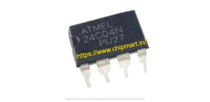
AT24CO4
Features
Low and Standard Voltage Operation: 2.7 (VCC = 2.7 to 5.5 V) and 1.8 (VCC = 1.8 to 5.5 V)
?128 x 8, 256 x 8, 512 x 8, 1024 x 8, or 2048 x 8 internal organisation (16K)
Bidirectional Data Transfer Protocol, Schmidt Trigger, Filtered Inputs for Noise Suppression, Two-wire Serial Interface, and Compatibility at 100 kHz (1.8V) and 400 kHz (2.7V, 5V)
8-byte page (1K, 2K), 16-byte page, Write Protect Pin for Hardware Data Protection (4K, 8K, 16K) Writing Styles
?High-reliability? Endurance: 1 Million Write Cycles? Data Retention: 100 Years ?Partial Page Writes Allowed ?Self-timed Write Cycle (5 ms max)
?Automotive Grade and Lead-free/Halogen-free Devices Available
?5-lead SOT23,8-lead TSSOP,8-lead PDIP,8-lead JEDEC SOIC,8-lead MAP, and 8-ball dBGA2 Packages
?Die Sales: Bumped Wafers, Waffle Packs, and Wafer Forms
The 1024/2048/4096/8192/16384 bits of serial electrically erasable and programmable read-only memory (EEPROM) provided by the AT24C01A/02/04/08A/16A are structured as 128/256/512/1024/2048 words of 8 bits each. The gadget is designed with a variety of industrial and business applications in mind, where low-power and low-voltage functioning are crucial. The AT24C01A/02/04/08A/16A is accessible through a Two-wire serial interface and is offered in compact 8-lead PDIP, 8-lead JEDEC SOIC, 8-lead MAP, 5-lead SOT23 (AT24C01A/AT24C02/AT24C04), 8-lead TSSOP, and 8-ball dBGA2 packages. There are other variants of the complete series in 2.7V (2.7V to 5.5V) and 1.8V (1.8V to 5.5V) voltage ranges.
AT25640B-SSHL-T
The Serial Electrically-Erasable Programmable Read-Only Memory (EEPROM) on the Atmel? AT25320B/640B has 32,768-/65,536-bits and is divided into 4,096/8,192 words with 8 bits each. The device is prepared for usage in a wide range of industrial and commercial settings where moderate and low-voltage functioning are critical requirements. The 8-lead JEDEC SOIC, 8-lead TSSOP, 8-lead UDFN, 8-lead XDFN, and 8-ball VFBGA packages for the AT25320B/640B are available in compact sizes. A 3-wire interface made up of Serial Data Input (SI), Serial Data Output (SO), and Serial Clock is used to access and enable the AT25320B/640B. (SCK). No further erase cycle is necessary before Write since every programming cycle is fully self-timed. Programming one of the four blocks of write security into the status register activates block write protection. For added data security, separate instructions for programme enable and programme disable are given. The WP pin offers hardware data protection to guard against unintentional write attempts to the status register. Any serial communication can be halted using the HOLD pin without having to restart the serial sequence.