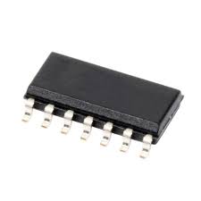
ADE7858ACPZ
The ADE7854/ADE7858/ADE7868/ADE7878 are high accuracy,
3-phase electrical energy measurement ICs with serial interfaces
and three flexible pulse outputs. The ADE78xx devices incorporate
second-order sigma-delta (Σ-∆) analog-to-digital converters
(ADCs), a digital integrator, reference circuitry, and all of the
signal processing required to perform total (fundamental and
harmonic) active, reactive (ADE7878, ADE7868, and
ADE7858), and apparent energy measurement and rms calculations, as well as fundamental-only active and reactive energy
measurement (ADE7878) and rms calculations. A fixed function
digital signal processor (DSP) executes this signal processing.
The DSP program is stored in the internal ROM memory
ADG407BN
1. Extended Signal Range.
2. The ADG406/ADG407/ADG426 are fabricated on an
enhanced LC2
MOS process giving an increased signal
range which extends to the supply rails.
3. Low Power Dissipation.
4. Low RON.
5. Single/Dual Supply Operation.
6. Single Supply Operation.
7. For applications where the analog signal is unipolar, the
ADG406/ADG407/ADG426 can be operated from a single
rail power supply. The parts are fully specified with a single
12 V power supply and remain functional with single
supplies as low as 5 V
ADG409BR
The ADG408/ADG409 are monolithic CMOS analog multiplexers
comprising eight single channels and four differential channels,
respectively. The ADG408 switches one of eight inputs to a
common output as determined by the 3-bit binary address lines
A0, A1, and A2. The ADG409 switches one of four differential
inputs to a common differential output, as determined by the
2-bit binary address lines A0 and A1. An EN input on both devices
is used to enable or disable the device. When the device is disabled,
all channels are switched off.
ADG413BR
The ADG411, ADG412, and ADG413 are monolithic CMOS
devices comprising four independently selectable switches.
They are designed on an enhanced LC2
MOS process which
provides low power dissipation yet gives high switching speed
and low on resistance.
The on resistance profile is very flat over the full analog input
range ensuring excellent linearity and low distortion when
switching audio signals. Fast switching speed coupled with high
signal bandwidth also make the parts suitable for video signal
switching. CMOS construction ensures ultralow power
dissipation, making the parts ideally suited for portable and
battery-powered instruments
ADG444BR
The ADG441, ADG442, and ADG444 are monolithic CMOS
devices that comprise of four independently selectable switches.
They are designed on an enhanced LC2
MOS process that
provides low power dissipation yet gives high switching speed
and low on resistance.
The on resistance profile is very flat over the full analog input
range, which ensures good linearity and low distortion when
switching audio signals. High switching speed also makes the
parts suitable for video signal switching. CMOS construction
ensures ultralow power dissipation, making the parts ideally
suited for portable and battery-powered instruments. The
ADG441, ADG442, and ADG444 contain four independent
SPST switches. Each switch of the ADG441 and ADG444 turns
on when a logic low is applied to the appropriate control input.
The ADG442 switches are turned on with logic high on the
appropriate control input. The ADG441 and ADG444 switches
differ in that the ADG444 requires a 5 V logic power supply
that is applied to the VL pin. The ADG441 and ADG442 do not
have a VL pin, the logic power supply is generated internally by
an on-chip voltage generator.


