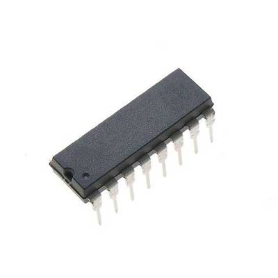
CD74HC40105E
This device contains two independent 4-input AND
gates. Each gate performs the Boolean function
Y = A ? B ? C ? D in positive logic.
Buffered inputs
? Wide operating voltage range: 2 V to 6 V
? Wide operating temperature range:
-55?C to 125?C
? Supports fanout up to 10 LSTTL loads
? Significant power reduction compared to LSTTL
logic IC
CD74HC4017E
The ?HC4017 is a high speed silicon gate CMOS 5-stage
Johnson counter with 10 decoded outputs. Each of the
decoded outputs is normally low and sequentially goes high
on the low to high transition clock period of the 10 clock
period cycle. The CARRY (TC) output transitions low to high
after OUTPUT 10 goes from high to low, and can be used in
conjunction with the CLOCK ENABLE (CE) to cascade
several stages. The CLOCK ENABLE input disables
counting when in the high state. A RESET (MR) input is also
provided which when taken high sets all the decoded
outputs, except ?0?, low.
The device can drive up to 10 low power Schottky equivalent
loads.
CD74HC540E
The ?HC540 and CD74HCT540 are Inverting Octal
Buffers and Line Drivers with Three-State Outputs
and the capability to drive 15 LSTTL loads.
The ?HC541 and ?HCT541 are Noninverting Octal
Buffers and Line Drivers with Three-State Outputs
that can drive 15 LSTTL loads. The Output Enables
(OE1) and (OE2) control the Three-State Outputs. If
either OE1 or OE2 is HIGH the outputs will be in the
high impedance state. For data output OE1 and OE2
both must be LOW.
CD74HC564E
The ?HC534, ?HCT534, ?HC564, and ?HCT564 are
high speed Octal D-Type Flip-Flops manufactured
with silicon gate CMOS technology. They possess the
low power consumption of standard CMOS integrated
circuits, as well as the ability to drive 15 LSTTL loads.
Due to the large output drive capability and the threestate feature, these devices are ideally suited for
interfacing with bus lines in a bus organized system.
The two types are functionally identical and differ only
in their pinout arrangements
CD74HCT08E
? LSTTL input logic compatible
? VIL(max) = 0.8 V, VIH(min) = 2 V
? CMOS input logic compatible
? II
? 1 ?A at VOL, VOH
? Buffered inputs
? 4.5 V to 5.5 V operation
? Wide operating temperature range:
-55?C to 125?C
? Supports fanout up to 10 LSTTL loads
? Significant power reduction compared to LSTTL
logic ICs
CD74HCT123E
The ?HC123, ?HCT123, CD74HC423 and CD74HCT423 are
dual monostable multivibrators with resets. They are all
retriggerable and differ only in that the 123 types can be
triggered by a negative to positive reset pulse; whereas the
423 types do not have this feature. An external resistor (RX)
and an external capacitor (CX) control the timing and the
accuracy for the circuit. Adjustment of Rx and CX provides a
wide range of output pulse widths from the Q and Q
terminals. Pulse triggering on the A and B inputs occur at a
particular voltage level and is not related to the rise and fall
times of the trigger pulses.
Once triggered, the output pulse width may be extended by
retriggering inputs A and B. The output pulse can be
terminated by a LOW level on the Reset (R) pin. Trailing
edge triggering (A) and leading edge triggering (B) inputs
are provided for triggering from either edge of the input
pulse. If either Mono is not used each input on the unused
device (A, B, and R) must be terminated high or low
CD74HCT123M
The ?HC123, ?HCT123, CD74HC423 and CD74HCT423 are
dual monostable multivibrators with resets. They are all
retriggerable and differ only in that the 123 types can be
triggered by a negative to positive reset pulse; whereas the
423 types do not have this feature. An external resistor (RX)
and an external capacitor (CX) control the timing and the
accuracy for the circuit. Adjustment of Rx and CX provides a
wide range of output pulse widths from the Q and Q
terminals. Pulse triggering on the A and B inputs occur at a
particular voltage level and is not related to the rise and fall
times of the trigger pulses.
Once triggered, the output pulse width may be extended by
retriggering inputs A and B. The output pulse can be
terminated by a LOW level on the Reset (R) pin. Trailing
edge triggering (A) and leading edge triggering (B) inputs
are provided for triggering from either edge of the input
pulse. If either Mono is not used each input on the unused
device (A, B, and R) must be terminated high or low.
CD74HCT132M
LSTTL input logic compatible
? VIL(max) = 0.8 V, VIH(min) = 2 V
? CMOS input logic compatible
? II
? 1 ?A at VOL, VOH
? Buffered inputs
? 4.5 V to 5.5 V operation
? Wide operating temperature range:
?55?C to 125?C
? Supports fanout up to 10 LSTTL loads
? Significant power reduction compared to LSTTL
logic ICs
CD74HCT166E
The ?HC166 and ?HCT166 8-bit shift register is fabricated
with silicon gate CMOS technology. It possesses the low
power consumption of standard CMOS integrated circuits,
and can operate at speeds comparable to the equivalent low
power Schottky device.
The ?HCT166 is functionally and pin compatible with the
standard ?LS166.
The 166 is an 8-bit shift register that has fully synchronous
serial or parallel data entry selected by an active LOW Parallel
Enable (PE) input. When the PE is LOW one setup time before
the LOW-to-HIGH clock transition, parallel data is entered into
the register. When PE is HIGH, data is entered into the internal
bit position Q0 from Serial Data Input (DS), and the remaining
bits are shifted one place to the right (Q0 ? Q1 ? Q2, etc.)
with each positive-going clock transition. For expansion of the
register in parallel to serial converters, the Q7 output is connected to the DS input of the succeeding stage


