


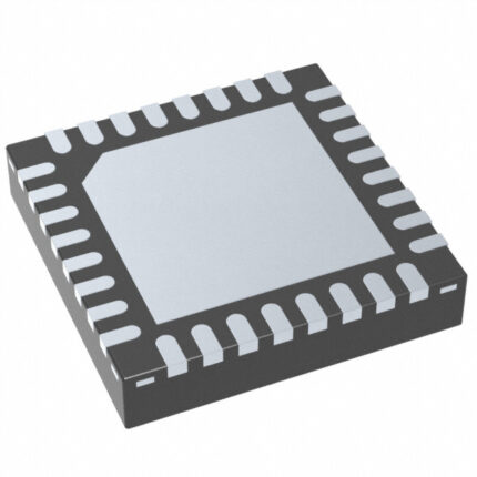
TPS54332DDA
₹91.00
Features of TPS54332DDA
- An input voltage range of 3.5 to 28 volts
- Output voltage is variable down to 0.8 V
- An integrated 80-m high-side MOSFET can handle an output current of up to 3.5 A continuously.
- High efficiency with pulse-skipping Eco-ModeTM at light loads
- Fixed switching frequency of 1 MHz
- A typical shutdown quiescent current of 1 A
- Variable slow-start restricts inrush currents
- Adjustable threshold for UVLO
- Protection from overvoltage transients
- Protection against thermal shutdown, frequency foldback, and cycle-by-cycle current limits
- Available in an 8-Pin SOIC Power PADTM package with thermal enhancement
- Supported by the tool WEBENCHTM
Applications of TPS54332DDA
- Usage by consumers, including set-top boxes, CPE devices, LCD displays, peripherals, and battery chargers
- Automotive and commercial power supply
- Distributed power systems with voltages of 5V, 12V, and 24V
2702 in stock
Description of TPS54332DDA
The TPS54332DDA is a non-synchronous buck converter with a low-RDS(on) high-side MOSFET that operates at 28 V and 3.5 A. An automatic pulse-skipping Eco-Mode feature is turned on to increase efficiency under light loads. Furthermore, the device can be used in battery-powered applications thanks to the 1-A shutdown supply current.
The external compensation calculations are made easier and the component count is decreased when using current mode control with internal slope compensation, which also permits the use of ceramic output capacitors.
The input under-voltage lockout’s hysteresis is controlled by a resistor divider. Voltage overshoots during startup and transient situations are restricted by an overvoltage transient protection circuit.
In the event of an overload condition, a cycle-by-cycle current limit system, frequency foldback, and thermal shutdown protect the device and the load. The 8-pin SOIC Power PADTM packaging for the TPS54332DDA is available.


MAECENAS IACULIS
Vestibulum curae torquent diam diam commodo parturient penatibus nunc dui adipiscing convallis bulum parturient suspendisse parturient a.Parturient in parturient scelerisque nibh lectus quam a natoque adipiscing a vestibulum hendrerit et pharetra fames nunc natoque dui.
ADIPISCING CONVALLIS BULUM
- Vestibulum penatibus nunc dui adipiscing convallis bulum parturient suspendisse.
- Abitur parturient praesent lectus quam a natoque adipiscing a vestibulum hendre.
- Diam parturient dictumst parturient scelerisque nibh lectus.
Scelerisque adipiscing bibendum sem vestibulum et in a a a purus lectus faucibus lobortis tincidunt purus lectus nisl class eros.Condimentum a et ullamcorper dictumst mus et tristique elementum nam inceptos hac parturient scelerisque vestibulum amet elit ut volutpat.
Related products
LNK420EG IC – Power Integrations – LED Driver Off Line Switcher IC

TNY267PN IC – Power Integrations Off Line Switcher IC


TNY280PN IC – Power Integrations AC/DC Converter IC
TNY280PN IC - TinySwitch?-III energy-efficient, off-line switcher with enhanced flexibility and extended power range that incorporates a 700V power MOSFET, oscillator, high-voltage switched current source, current limit (user selectable), and thermal shutdown circuitry. The IC family uses an ON/OFF control scheme and offers a design flexible solution with a low system cost and extended power capability. The application includes chargers/adapters for cell/cordless phones, PDAs, digital cameras, MP3/portable audio, shavers, PC standby and other auxiliary supplies, DVD/PVR, and other low-power set-top decoders, supplies for appliances, industrial systems, and metering. ON/OFF control provides constant efficiency down to a very light load and it is ideal for mandatory CEC regulations and 1W PC standby requirements. Very low component count enhances reliability and enables a single-sided printed circuit board layout. High bandwidth provides fast turn-on with no overshoot and excellent transient load response.

TOP227YN IC – Power Integrations – Off Line Switcher IC

TOP245YN IC – Power Integrations – Off Line Switcher IC
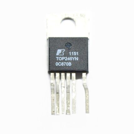
TOP246YN IC – Power Integrations – Off Line Switcher IC


Reviews
There are no reviews yet.