

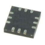

TLV62585RWT
₹26.00
Features of TLV62585RWT
- 95% maximum efficiency
- 56 m / 32 m low RDS(ON) power switches
- Range of input voltages: 2.5 to 5.5 V
- Variable output voltage between 0.6 and VIN
- Efficiency in power saving mode for light loads
- Maximum duty cycle for minimal dropout
- Operating quiescent current of 35 A
- Typical switching frequency of 1.5 MHz
- Short circuit defense (HICCUP)
- Discharge of output
- Excellent power output
- Thermal shut-down defense
- Available either a 1.6-mm x 1.6-mm SOT563 package or a 2-mm x 2-mm QFN package.
9000 in stock
Description of TLV62585RWT
A high-frequency synchronous step-down converter with great efficiency and a small solution size is the TLV62585RWT device. Switches integrated into the gadget can deliver output currents of up to 3 A. The converter operates in pulse width modulation (PWM) mode with a typical 1.5-MHz switching frequency while under medium to heavy loads.
To maintain high efficiency over the whole load current range, the device automatically enters Power Save Mode (PSM) when under light load. Less than 2 A of current are consumed during shutdown.
Compact solutions and few external components are made possible by the internal compensating circuit. During startup, an inbuilt soft start circuit regulates the inrush current.
There are also built-in functions such output discharge, short circuit protection, thermal shutdown protection, and power excellent. The device is offered in a 1.6-mm x 1-6-mm SOT563 packaging or a 2-mm x 2-mm QFN package.


MAECENAS IACULIS
Vestibulum curae torquent diam diam commodo parturient penatibus nunc dui adipiscing convallis bulum parturient suspendisse parturient a.Parturient in parturient scelerisque nibh lectus quam a natoque adipiscing a vestibulum hendrerit et pharetra fames nunc natoque dui.
ADIPISCING CONVALLIS BULUM
- Vestibulum penatibus nunc dui adipiscing convallis bulum parturient suspendisse.
- Abitur parturient praesent lectus quam a natoque adipiscing a vestibulum hendre.
- Diam parturient dictumst parturient scelerisque nibh lectus.
Scelerisque adipiscing bibendum sem vestibulum et in a a a purus lectus faucibus lobortis tincidunt purus lectus nisl class eros.Condimentum a et ullamcorper dictumst mus et tristique elementum nam inceptos hac parturient scelerisque vestibulum amet elit ut volutpat.
Related products
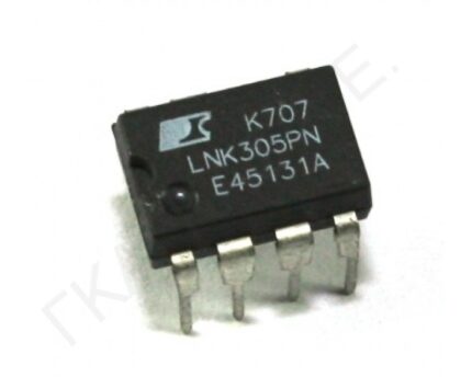
LNK305PN IC – Power Integrations – AC-DC Off Line Switcher IC
LNK420EG IC – Power Integrations – LED Driver Off Line Switcher IC

TNY266PN IC – Power Integrations Off Line Switcher IC

TNY267PN IC – Power Integrations Off Line Switcher IC
TNY268PN IC – Power Integrations Off Line Switcher with Low Power IC
TNY268PN IC - Low Power Off-Line Switcher - Power Integrations - DIP-8
The TNY268PN integrates a 700V power MOSFET, oscillator, high voltage switched current source, current limit, and thermal shutdown circuitry onto a monolithic device. The start-up and operating power are derived directly from the voltage on the DRAIN pin, eliminating the need for a bias winding and associated circuitry. In addition, the TNY268PN incorporates auto-restart, line under voltage sense, and frequency jittering. An innovative design minimizes audio frequency components in the simple ON/OFF control scheme to practically eliminate audible noise with standard taped/varnished transformer construction. The fully integrated auto-restart circuit safely limits output power during fault conditions such as output short circuits or open loop, reducing component count and secondary feedback circuitry cost.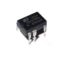

TOP224YN IC – Power Integrations – Off Line Switcher IC


Reviews
There are no reviews yet.