
")
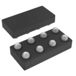
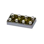

SN74LVC2G241YZPR
₹8.00
Characteristics of the SN74LVC2G241YZPR
- Texas Instruments offers it.
- Packaged in NanoFreeTM
- Supports Operation at 5-V VCC
- Voltage Acceptance to 5.5 V for Inputs
- 4.1 ns maximum tpd at 3.3 V
- Low Power Consumption, ICC at most 10-A
- 3.3 V, 24-mA Output Drive
- At VCC = 3.3 V, TA = 25?C, the typical VOLP (Output Ground Bounce) is 0.8 V. Standard VOHV (Output VOH Undershoot)
- VCC = 3.3 V, TA = 25?C, >2 V
- Live Insertion, Partial-Power-Down Mode, and Back-Drive Protection are supported by Ioff.
- Can Translate Inputs From a Max of 5.5 V Down to the VCC Level When Used as a Down Translator
- Performance of the Latch-Up Exceeds 100 mA Per JESD 78, Class II
- JESD 22 Exceeds ESD Protection
Applications of SN74LVC2G241YZPR
- A/V Receivers
- Home theatre systems with Blu-ray players
- DVD players and recorders
- Desktop or laptop computers
- Internet or digital radio players
- Digital cameras with video (DVC)
- Integrated PCs
- Personal Navigation Systems (GPS)
- Devices for mobile internet
- ?Front-ends for network projectors
- Media Players Portables
- Pro audio mixers
3000 in stock
Description of SN74LVC2G241YZPR
The operating range of this dual buffer and line driver is 1.65-V to 5.5-V VCC.
Clock drivers, bus-oriented receivers and transmitters, 3-state memory-address drivers, and clock drivers are among the applications for which the SN74LVC2G241 chip is specifically intended to enhance performance and density.
A significant development in SN74LVC2G241YZPR packaging ideas is the NanoFree package technology, which uses the die as the package.
Two 1-bit line drivers with distinct output-enable (1OE, 2OE) inputs make up the SN74LVC2G241 device. The device transfers data from the A inputs to the Y outputs when 1OE and 2OE are both low. The outputs are in the high-impedance state when 1OE is high and 2OE is low.
Pullup and pulldown resistors should be used to connect OE to VCC and GND, respectively, to assure the high-impedance state during power-up and power-down. The minimum value of the resistor depends on the driver’s ability to source or sink current.
This device meets the requirements for Ioff applications involving partial power reduction. When a device is turned off, the Ioff circuitry turns off the outputs to stop potentially harmful current backflow through the device.


MAECENAS IACULIS
Vestibulum curae torquent diam diam commodo parturient penatibus nunc dui adipiscing convallis bulum parturient suspendisse parturient a.Parturient in parturient scelerisque nibh lectus quam a natoque adipiscing a vestibulum hendrerit et pharetra fames nunc natoque dui.
ADIPISCING CONVALLIS BULUM
- Vestibulum penatibus nunc dui adipiscing convallis bulum parturient suspendisse.
- Abitur parturient praesent lectus quam a natoque adipiscing a vestibulum hendre.
- Diam parturient dictumst parturient scelerisque nibh lectus.
Scelerisque adipiscing bibendum sem vestibulum et in a a a purus lectus faucibus lobortis tincidunt purus lectus nisl class eros.Condimentum a et ullamcorper dictumst mus et tristique elementum nam inceptos hac parturient scelerisque vestibulum amet elit ut volutpat.
Related products


Reviews
There are no reviews yet.