

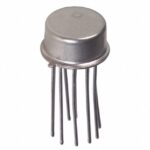
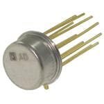
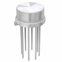

AD536AJH
₹3,000.00
The AD536A is a complete monolithic integrated circuit that performs the true RMS-to-dc conversion. It offers performance comparable to or superior to that of hybrid or modular units costing much more. The AD536A directly computes the true RMS value of any complex input waveform containing ac and dc components.
Mfr. No: AD536AJH
Mfr.:Analog Devices
Description: Power Management Specialised – PMIC RMS/DC CONVERTER IC
Datasheet: AD536AJH Datasheet (PDF)
FEATURES – AD536AJH
- True rms-to-dc conversion
- Laser trimmed to high accuracy
?0.2% maximum error (AD536AK)
?0.5% maximum error (AD536AJ) - Wide response capability
- Computes rms of ac and dc signals
450 kHz bandwidth: V rms > 100 mV
2 MHz bandwidth: V rms > 1 V
Signal crest factor of 7 for 1% error - dB output with 60 dB range
- Low power: 1.2 mA quiescent current
- Single- or dual-supply operation
- Monolithic integrated circuit
?55?C to +125?C operation (AD536AS)
AD536AJH – A crest factor compensation scheme allows measurements with 1% error at crest factors up to 7. The wide bandwidth of the device extends the measurement capability to 300 kHz with less than 3 dB errors for signal levels greater than 100 mV.
An important feature of the AD536A, not previously available in rms converters, is an auxiliary dB output pin. The logarithm of the rms output signal is brought out to a separate pin to allow the dB conversion, with a useful dynamic range of 60 dB. Using an externally supplied reference current, the 0 dB level can be conveniently set to correspond to any input level from 0.1 V to 2 V rms.
The AD536A is laser trimmed to minimize input and output offset voltage, to optimize positive and negative waveform symmetry (dc reversal error), and to provide full-scale accuracy at 7 V rms. As a result, no external trims are required to achieve the rated unit accuracy.
The input and output pins are fully protected. The input circuitry take overload voltages well beyond the supply levels. Loss of supply voltage with the input connected to external circuitry does not cause the device to fail. The output is short-circuit protected.
The AD536A is available in two accuracy grades (J and K) for commercial temperature range (0?C to 70?C) applications, and one grade (S) rated for the ?55?C to +125?C extended range. The AD536AK offers a maximum total error of ?2 mV ? 0.2% of reading, while the AD536AJ and AD536AS have maximum errors of ?5 mV ? 0.5% of reading. All three versions are available in a hermetically sealed 14-lead DIP or a 10-pin TO-100 metal header package. The AD536AS is also available in a 20-terminal leadless hermetically sealed ceramic chip carrier.
The AD536A computes the true root-mean-square level of a complex ac (or ac plus dc) input signal and provides an equivalent dc output level. The true rms value of a waveform is a more useful quantity than the average rectified value because it relates directly to the power of the signal. The rms value of a statistical signal also relates to its standard deviation.
An external capacitor is required to perform measurements to the fully specified accuracy. The value of this capacitor determines the low frequency ac accuracy, ripple amplitude, and settling time. The AD536A operates equally well from split supplies or a single supply with total supply levels from 5 V to 36 V. With 1 mA quiescent supply current, the device is well suited for a wide variety of remote controllers and battery-powered instruments.


MAECENAS IACULIS
Vestibulum curae torquent diam diam commodo parturient penatibus nunc dui adipiscing convallis bulum parturient suspendisse parturient a.Parturient in parturient scelerisque nibh lectus quam a natoque adipiscing a vestibulum hendrerit et pharetra fames nunc natoque dui.
ADIPISCING CONVALLIS BULUM
- Vestibulum penatibus nunc dui adipiscing convallis bulum parturient suspendisse.
- Abitur parturient praesent lectus quam a natoque adipiscing a vestibulum hendre.
- Diam parturient dictumst parturient scelerisque nibh lectus.
Scelerisque adipiscing bibendum sem vestibulum et in a a a purus lectus faucibus lobortis tincidunt purus lectus nisl class eros.Condimentum a et ullamcorper dictumst mus et tristique elementum nam inceptos hac parturient scelerisque vestibulum amet elit ut volutpat.
Related products
DPA422PN
LNK364 IC – Low Power Offline Switcher IC
TOP222YN IC – Power Integrations – Off Line Switcher IC
TOP223YN IC – Power Integrations – Off Line Switcher IC

TOP227YN IC – Power Integrations – Off Line Switcher IC

TOP248YN IC – Power Integrations – Off Line Switcher IC


Reviews
There are no reviews yet.