BD6221F-E2
Basic Information
Full bridge drivers, or H-bridges, are what are used in brush motor applications. Each IC has an operating voltage range of 6V to 15V and a maximum output current of 2A. The output stage's MOS transistors enable PWM speed control. Motor driver ICs that have been discontinued can be directly replaced thanks to the inbuilt VREF voltage control mechanism. Low-power consumption designs are made possible by these incredibly efficient H-bridge driver ICs.
Features
Built-in Selectable Features Cross-Conduction Prevention Circuit, OCP, OVP, TSD, and UVLO Protection Circuits, One Channel or Two Channels Configuration, VREF Voltage Setting Pin Enables PWM Duty Control, and One or Two Channels Configuration.
Key Particulars
Maximum Output Current: 0.5A, 1.0A, 2.0A;
Output ON-Resistance: 1.5;
PWM Input Frequency Range: 20kHz to 100kHz;
Standby Current: 0A;
Supply Voltage Range: 18V(Max); (Typ)
-40?C to 85?C is the operating temperature range.
Applications
VTR, CD/DVD players, audiovisual gear, optical disc drives, PC add-ons, and OA equipment
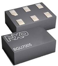
BGU7005
Benefits and features of BGU7005
- Covers the entire GNSS L1 range, 1559 to 1610 MHz
- Noise figure (NF) is equal to 0.85 dB.
- Increase 16.5 dB
- A lot of input Pi(1dB), or 1 dB compression point, is 11 dBm.
- High IP3i out of band of 9 dBm
- 1.5 to 3.1 volts is the supply voltage.
- Consumption of current in power-saving mode is 1 A.
- Optimized performance at 4.5 mA, a low supply current
- Output matching that is integrated
- Only needs one supply decoupling capacitor and one input matching inductor.
- Decoupled DC input and output
- All pins have ESD protection (HBM > 2 kV).
- Temperature-stabilized bias included for simple design
- Small leadless 6-pin package 1.45 mm, 1 mm, and 0.5 mm
- Transit frequency of 110 GHz using SiGe:C technology
BP3122
The BP3122 is a high precision primary-side feedback and regulation controller for LED lighting that functions in constant current control mode and is designed to work in inductor current discontinuous conduction mode, making it particularly ideal for fly back converters with universal input. The system's output power should be less than 5W.
The BP3122 contains a 650V power MOSFET. The secondary sensing and feedback circuit has been deleted since the adoption of main sense and feedback control technology. The looping compensatory components are likewise deleted while the overall operating conditions remain stable. It employs patent-pending source driver design and demagnetization detecting technology, has a very low operating current, and does not require an extra winding for measuring output current and powering the device. Because of the low component counts
Using the innovative high precise current sensing technology, the BP3122 achieves 5% LED current accuracy as well as good line and load control.
The BP3122 includes several protective features such as LED open/short circuit protection, CS resistor short circuit protection, over-temperature protection, and VCC under voltage protection.
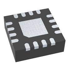
BQ24230RGT
Features of BQ24230
- Up to 500 mA of charge current is supported, and a current monitoring output is provided (ISET)
- For wall adapters, programmable input current limit of up to 500 mA
- Termination Current With Programmability (bq24232)
- Pre-charge and fast-charge safety timers that are programmable
- Short-Circuit, Thermal, and Reverse Current Protection
- Input NTC Thermistor
- Exclusive Start-Up Sequence Controls Inrush Current
- Charged/Done Status Indication, Good Power
- 16-Lead 3 mm x 3 mm Small QFN Package
- With Overvoltage Protection and a 28-V Input Rating
- Function of Integrated Dynamic Power-Path Management (DPPM) Powers the System and Charges the Battery Separately and Concurrently
- ? USB Charger Fully Compliant - Selectable Maximum Input Current of 100 mA and 500 mA - The USB-IF standard is ensured by the 100-mA maximum current limit. - Protection Against Subpar USB Sources using Input-based Dynamic Power Management (VIN- DPM)
- Bluetooth? Devices
- Low-Power Handheld Devices
BQ25100YFP
Features of BQ25100YFP
- Adjustable thresholds for termination and pre-charge
- Dynamic input voltage power management
- ISET short detection and OUT short-circuit prevention
- 10 hour fixed safety timer
- 1% accuracy in charge voltage
- 10% accuracy in charge current
- Green products without Sb or Br
- Recharge - 1% Accuracy in Charge Voltage - 10 percent charge current accuracy - Supports 10 mA to 250 mA charge current applications. - Supports a 1-mA charge termination current minimum -Maximum 75 nA Ultra Low Battery Output Leakage Current
- Adjustable Pre-charge and Termination Threshold
- 4.35V with bq25100H/01H and 4.30V with bq25100A for high voltage chemistry support
- Fitness Equipment
- A smart watch
- Headsets with Bluetooth?
- Low-Power Portable Electronics
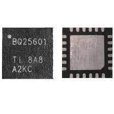
BQ25601RTW
Features of BQ25601RTW
- High-efficiency, 1.5 MHz, synchronous switch-mode buck charger - 92% charge efficiency at 2 A from 5 V input - Optimized for USB voltage input (5 V)
- Supports USB OTG - Boost converter with up to 1.2 A output - 92% boost efficiency at 1 A output - Accurate constant current (CC) limit - Soft-start up to 500 ?F capacitive load - Output short-circuit protection
- Single input to support USB input and high voltage adapters - Support 3.9 V to 13.5 V input voltage range with 20 V absolute maximum input voltage rating - Maximum power tracking by input voltage limit up to 4.6 V (VINDPM) - VINDPM threshold automatically tracks battery voltage - Auto detect USB SDP, DCP and non-standard adapters
- 200 nS fast turn-off of optional external OVPFET standing input voltage up to 40?V
- High battery discharge efficiency with 19.5 m? battery discharge MOSFET
- High integration includes all MOSFETs, current sensing, and loop compensation
- 58 ?A low battery leakage current with system voltage standby
- EPOS, portable speakers, e-cigarettes
- Portable internet devices and accessories
CA3102E Dual High Frequency Differential Amplifier IC DIP-14
The CA3102 consists of two independent differential amplifiers with associated constant current transistors on a common monolithic substrate. The six transistors which comprise the amplifiers are general purpose devices which exhibit low 1/f noise and a value of fT in excess of 1GHz. These features make the CA3102 useful from DC to 500MHz. Bias and load resistors have been omitted to provide maximum application flexibility. The monolithic construction of the CA3102 provides close electrical and thermal matching of the amplifiers
CA3130 CMOS Op-Amp IC DIP-8
The CA3130 are op amps that combine the advantage of both CMOS and bipolar transistors. Gate-protected P-Channel MOSFET (PMOS) transistors are used in the input circuit to provide very-high-input impedance, very-low-input current, and exceptional speed performance. The use of PMOS transistors in the input stage results in common-mode input-voltage capability down to 0.5V below the negative-supply terminal, an important attribute in single-supply applications. A CMOS transistor-pair, capable of swinging the output voltage to within 10mV of either supply-voltage terminal (at very high values of load impedance), is employed as the output circuit.
CA3140 BiMOS Op-Amp IC DIP-8
The CA3140 are integrated circuit operational amplifiers that combine the advantages of high voltage PMOS transistors with high voltage bipolar transistors on a single monolithic chip. The CA3140 BiMOS operational amplifiers feature gate protected MOSFET (PMOS) transistors in the input circuit to provide very high input impedance, very low input current, and high speed performance. The CA3140 operate at supply voltage from 4V to 36V (either single or dual supply). These operational amplifiers are internally phase compensated to achieve stable operation in unity gain follower operation, and additionally, have access terminal for a supplementary external capacitor if additional frequency roll-off is desired. Terminals are also provided for use in applications requiring input offset voltage nulling.


