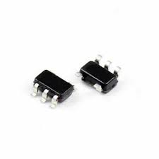
MAX825
The MAX823/MAX824/MAX825* microprocessor (?P)
supervisory circuits combine reset output, watchdog,
and manual reset input functions in 5-pin SOT23 and
SC70 packages. They significantly improve system reliability and accuracy compared to separate ICs or discrete
components. The MAX823/MAX824/MAX825 are specifically designed to ignore fast transients on VCC.
Seven preprogrammed reset threshold voltages are
available (see Reset Threshold Table). All three devices
have an active-low reset output, which is guaranteed to
be in the correct state for VCC down to 1V. The MAX823
also offers a watchdog input and manual reset input.
The MAX824 offers a watchdog input and a complementary active-high reset. The MAX825 offers a manual
reset input and a complementary active-high reset. The
Selector Guide explains the functions offered in this
series of parts
MAX845ESA+
The MAX845 provides an isolated power supply small
enough to fit in thin PCMCIA cards and space-sensitive
applications. It drives a low-profile center-tapped transformer primary from a 5V or 3.3V DC power supply. The
secondary can be wound to provide any isolated positive or negative voltage at powers up to 750mW.
The MAX845 consists of an oscillator followed by a toggle flip-flop. The flip-flop generates two 50% duty-cycle
square waves, which are complementary at half the
oscillator frequency (450kHz, min). These two signals
drive the ground-referenced N-channel power switches. Internal circuitry ensures break-before-make action
between the two switches.
MAX856CSA
The MAX856?MAX859 are high-efficiency, CMOS, stepup, DC-DC switching regulators for small, low input voltage or battery-powered systems. The MAX856/MAX858
accept a positive input voltage between 0.8V and VOUT
and convert it to a higher, pin-selectable output voltage of
3.3V or 5V. The MAX857/MAX859 adjustable versions
accept 0.8V to 6.0V input voltages and generate higher
adjustable output voltages in the 2.7V to 6.0V range.
Typical efficiencies are greater than 85%. Typical quiescent supply current is 25?A (1?A in shutdown)
MAX856ESA
The MAX856?MAX859 are high-efficiency, CMOS, stepup, DC-DC switching regulators for small, low input voltage or battery-powered systems. The MAX856/MAX858
accept a positive input voltage between 0.8V and VOUT
and convert it to a higher, pin-selectable output voltage of
3.3V or 5V. The MAX857/MAX859 adjustable versions
accept 0.8V to 6.0V input voltages and generate higher
adjustable output voltages in the 2.7V to 6.0V range.
Typical efficiencies are greater than 85%. Typical quiescent supply current is 25?A (1?A in shutdown).
MAX861ESA
The MAX860/MAX861 charge-pump voltage converters
invert input voltages ranging from 1.5V to 5.5V, or
double input voltages ranging from 2.5V to 5.5V.
Because of their high switching frequencies, these
devices use only two small, low-cost capacitors. Their
50mA output makes switching regulators unnecessary,
eliminating inductors and their associated cost, size,
and EMI. Greater than 90% efficiency over most of the
load-current range, combined with a typical operating
current of only 200?A (MAX860), provides ideal performance for both battery-powered and board-level voltage-conversion applications.
MAX873BESA
The MAX873/MAX875/MAX876 precision 2.5V, 5V, and
10V references offer excellent accuracy and very low
power consumption. Extremely low temperature drift
combined with excellent line and load regulation permit
stable operation over a wide range of electrical and environmental conditions. Operation for the MAX873 is guaranteed with a 4.5V supply, making the part ideal in
systems running from a 5V ?10% supply. Low 10Hz to
1kHz noise?typically 3.8?VRMS, 9?VRMS, and 18?VRMS,
respectively, for the MAX873, MAX875, MAX876?make
the parts suitable for 12-bit data-acquisition systems.
MAX882CSA
The MAX882/MAX883/MAX884 linear regulators maximize battery life by combining ultra-low supply currents
and low dropout voltages. They feature 200mA output
current capability at up to 125?C junction temperature
and come in a 1.5W SOIC package. The 1.5W package
(compared to 0.47W for standard SOIC packages)
allows a wider operating range for the input voltage and
output current. The MAX882/MAX883/MAX884 use a pchannel MOSFET pass transistor to maintain a low 11?A
(15?A max) supply current from no-load to the full
200mA output. Unlike earlier bipolar regulators, there are
no PNP base current losses that increase with output
current. In dropout, the MOSFET does not suffer from
excessive base currents that occur when PNP transistors
go into saturation. Typical dropout voltages are 220mV
at 5V and 200mA, or 320mV at 3.3V and 200mA.
MAX901AEPE
All comparators can be powered from separate analog
and digital power supplies or from a single combined supply voltage. The analog input common-mode range
includes the negative rail, allowing ground sensing when
powered from a single supply. The MAX900?MAX903
consume 18mW per comparator when powered from 5V.
The MAX900?MAX903 are equipped with independent
TTL-compatible latch inputs. The comparator output
states are held when the latch inputs are driven low. The
MAX901 provides the same performance as the
MAX900/MAX902/MAX903 with the exception of the
latches.
MAX902EPD
All comparators can be powered from separate analog
and digital power supplies or from a single combined supply voltage. The analog input common-mode range
includes the negative rail, allowing ground sensing when
powered from a single supply. The MAX900?MAX903
consume 18mW per comparator when powered from 5V.
The MAX900?MAX903 are equipped with independent
TTL-compatible latch inputs. The comparator output
states are held when the latch inputs are driven low. The
MAX901 provides the same performance as the
MAX900/MAX902/MAX903 with the exception of the
latches.
MAX902ESD
The MAX900?MAX903 high-speed, low-power, single/
dual/quad voltage comparators feature differential analog inputs and TTL-logic outputs with active internal pullups. Fast propagation delay (8ns typ at 5mV overdrive)
makes the MAX900?MAX903 ideal for fast A/D converters and sampling circuits, line receivers, V/F converters,
and many other data-discrimination applications.
All comparators can be powered from separate analog
and digital power supplies or from a single combined supply voltage. The analog input common-mode range
includes the negative rail, allowing ground sensing when
powered from a single supply. The MAX900?MAX903
consume 18mW per comparator when powered from 5V
MAX907CSA
The MAX907/MAX908/MAX909 are dual/quad/single,
high-speed, ultra-low-power voltage comparators
designed for use in systems powered from a single
5V supply; the MAX909 also accepts dual ?5V supplies. Their 40ns propagation delay (with 5mV input
overdrive) is achieved with a power consumption of
only 3.5mW per comparator. The wide input commonmode range extends from 200mV below ground (below
the negative supply rail for the MAX909) to within 1.5V
of the positive supply rail.
Because they are micropower, high-speed comparators that operate from a single 5V supply and include
built-in hysteresis, these devices replace a variety of
older comparators in a wide range of applications.


