
LT1521IST5
Dropout Voltage: 0.5V
n Output Current: 300mA
n Quiescent Current: 12?A
n No Protection Diodes Needed
n Adjustable Output from 3.8V to 20V
n Fixed Output Voltages: 3V, 3.3V, 5V
n Controlled Quiescent Current in Dropout
n Shutdown IQ = 6?A
n Reverse Battery Protection
n No Reverse Current
n Thermal Limiting

LT1785IS8
The LT?1785/LT1791 are half-duplex and full-duplex differential bus transceivers for RS485 and RS422 applications
which feature on-chip protection from overvoltage faults
on the data transmission lines. Receiver input and driver
output pins can withstand voltage faults up to ?60V with
respect to ground with no damage to the device. Faults
may occur while the transceiver is active, shut down or
powered off.
Data rates to 250kbaud on networks of up to 128 nodes
are supported. Controlled slew rates on the driver outputscontrol EMI emissions and improve data transmission integrity on improperly terminated lines. Drivers are
specified to operate with inexpensive cables as low as
72? characteristic impedance.
The LT1785A/LT1791A devices have ?fail-safe? receiver
inputs to guarantee a receiver output high for shorted, open
or inactive data lines. On-chip ESD protection eliminates
need for external protection devices.
The LT1785/LT1785A are available in 8-lead DIP and SO
packages and the LT1791/LT1791A in 14-lead DIP and
SO packages.

LTC1040CSW#DPR
The LTC?
1040 is a monolithic CMOS dual comparator
manufactured using Linear Technology?s enhanced
LTCMOSTM silicon gate process. Extremely low operating
power levels are achieved by internally switching the
comparator ON for short periods of time. The CMOS
output logic holds the output information continuously
while not consuming any power.
In addition to switching power ON, a switched output is
provided to drive external loads during the comparator?s
active time. This allows not only low comparator power,
but low total system power.

LTC1051CN8
The LTC?
1051/LTC1053 are high performance, low cost
dual/quad zero-drift operational amplifiers. The unique
achievement of the LTC1051/LTC1053 is that they integrate
on chip the sample-and-hold capacitors usually required
externally by other chopper amplifiers. Further, the
LTC1051/LTC1053 offer better combined overall DC and
AC performance than is available from other chopper
stabilized amplifiers with or without internal sample/hold
capacitors.
The LTC1051/LTC1053 have an offset voltage of 0.5?V,
drift of 0.01?V/?C, DC to 10Hz, input noise voltage typically
1.5?VP-P and typical voltage gain of 140dB. The slew rate
of 4V/?s and gain bandwidth product of 2.5MHz are
achieved with only 1mA of supply current per op amp

LTC1487CS8
The LTC?
1487 is an ultra-low power differential line transceiver designed with high impedance inputs allowing up to
256 transceivers to share a single bus. It meets the
requirements of RS485 and RS422. The LTC1487 features
output drivers with controlled slew rate, decreasing the
EMI radiated from the RS485 lines, and improving signal
fidelity with misterminated lines. The CMOS design offers
significant power savings without sacrificing ruggedness
against overload or ESD damage. Typical quiescent current is only 80?A while operating and 1?A in shutdown
LTC1755EGN
The LTC?
1487 is an ultra-low power differential line transceiver designed with high impedance inputs allowing up to
256 transceivers to share a single bus. It meets the
requirements of RS485 and RS422. The LTC1487 features
output drivers with controlled slew rate, decreasing the
EMI radiated from the RS485 lines, and improving signal
fidelity with misterminated lines. The CMOS design offers
significant power savings without sacrificing ruggedness
against overload or ESD damage. Typical quiescent current is only 80?A while operating and 1?A in shutdown.

LTC491CS
The LTC?
491 is a low power differential bus/line transceiver designed for multipoint data transmission standard
RS485 applications with extended common mode range
(12V to ?7V). It also meets the requirements of RS422.
The CMOS design offers significant power savings over its
bipolar counterpart without sacrificing ruggedness against
overload or ESD damage.
The driver and receiver feature three-state outputs, with
the driver outputs maintaining high impedance over the
entire common mode range. Excessive power dissipation
caused by bus contention or faults is prevented by a
thermal shutdown circuit which forces the driver outputs
into a high impedance state.
The receiver has a fail safe feature which guarantees a high
output state when the inputs are left open.
Both AC and DC specifications are guaranteed from 0?C to
70?C and 4.75V to 5.25V supply voltage range.

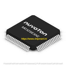
M031LE3AE
The Arm? Cortex?-M0 core with a 32-bit hardware multiplier/divider is the foundation of the NuMicro? M031/M032 series 32-bit microcontroller. It operates between -40?C and 105?C, operates at up to 48/72 MHz, and has a 1.8 3.6 V working voltage and 5 V I/O tolerance. For applications requiring a 1.8 V low-voltage interface connection with increased fast 2 MSPS conversion rate 12-bit ADC, comparators, and up to 24-ch96/144 MHz PWM control, the M031/M032 family offers a solution. For the voltages, power, and sensor readings, it offers quick and accurate data conversion, followed by quick reaction control for the external device. The Arm? Cortex?-M0 core with a 32-bit hardware multiplier/divider is the foundation of the NuMicro? M031/M032 series 32-bit microcontroller. It operates between -40?C and 105?C, operates at up to 48/72 MHz, and has a 1.8 3.6 V working voltage and 5 V I/O tolerance. For applications requiring a 1.8 V low-voltage interface connection with increased fast 2 MSPS conversion rate 12-bit ADC, comparators, and up to 24-ch96/144 MHz PWM control, the M031/M032 family offers a solution. For the voltages, power, and sensor readings, it offers quick and accurate data conversion, followed by quick reaction control for the external device.
The NuMicro? M031/M032 family is appropriate for a variety of uses, including: Laser Distance Meter Air Detector/Cleaner Mobile LCD Panel Controller IoT Sensing Device HMI Controller Micro Printer Gaming Keyboard and Mouse WPC Wireless Charger

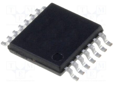
M24128-DRDW8TP/K
Features? of M24128-DRD
- Support for all I2C bus modes? 1 MHz/ 400 kHz/ 100 kHz
- Memory bank- An EEPROM with 128 Kbits (16 Kbytes)
- Page Size in Bytes: 64
- In addition Make a locked page.
- Wider range of temperatures and voltages?40 to 105 degrees Celsius; 1.7 to 5.5 volts
- Schmitt trigger inputs are used to filter noise.
- Cycle time for short writes- Byte Write in 4 milliseconds- Page Write in 4 milliseconds
- Express cycling stamina. -4,000,000 Write Cycles at 25 ?C, - 1,2,000,000 Write cycles at 85 ?C & ? 900 k Cycles of writing at 105 ?C
- Data storage- at 105 ?C for more than 50 years., 200 yr at 55 ?C
- ESD Defense (Human Body Model)? 4000 V
- Packing is- Halogen-free and RoHS compliant
- SMD/SMT mounting style
- Case/Package: TSSOP-8
- Interface types: I2C and 2-Wire
- Size of Memory: 128 kbit
- Arrangement: 16 k x 8
- Minimum Supply Voltage: 1.7 V
- Maximum Supply Voltage: 5.5 V
- 40 C for the minimum operating temperature
- 105 C is the maximum operating temperature.
- 1 MHz is the maximum clock frequency.
- Time to Access: 450 ns
- Retention of Data: 200 Years
- Maximum Supply Current: 2 mA
- The M24128-DRD series
- mandatory requirement: AEC-Q100
- Packaging: Cut Tape and Reel
- Maximum Active Read Current: 2 mA
- STMicroelectronics is a brand.
- 2 mA is the operating supply current.
- Voltage Range for Operating Supply: 1.8 to 5.5 V
- Type of Product: EEPROM

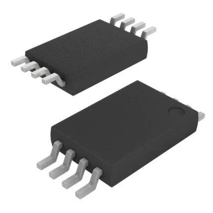
M24C32-WMN6
The M24C32 is a 32-Kbit I2C-compatible EEPROM (Electrically Erasable PROgrammable
Memory) organized as 4 K ? 8 bits.
The M24C32-W can operate with a supply voltage from 2.5 V to 5.5 V, the M24C32-R can
operate with a supply voltage from 1.8 V to 5.5 V, and the M24C32-F and M24C32-DF can
operate with a supply voltage from 1.7 V to 5.5 V, over an ambient temperature range of
-40 ?C / 85 ?C; while the M24C32-X can operate with a supply voltage from 1.6 V to 5.5 V
over an ambient temperature range of -20 ?C / 85 ?C.
The M24C32-D offers an additional page, named the Identification Page (32 byte). The
Identification Page can be used to store sensitive application parameters which can be
(later) permanently locked in Read-only mode.


