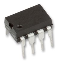
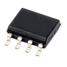
LT1004IS8-1.2
The micropower voltage reference is a
2-terminal bandgap reference diode designed to provide
high accuracy and excellent temperature characteristics
at very low operating currents. Optimization of the key
parameters in the design, processing and testing of
the device results in accuracy specifications previously
attainable only with selected units. Below is a distribution
plot of reference voltage for a typical lot of LT1004-1.2.
Virtually all of the units fall well within the prescribed
limits of ?4mV.
The LT1004 is a pin-for-pin replacement for the
LM185/LM385 series of references with improved accuracy specifications. More important, the LT1004 is an
attractive device for use in systems where accuracy was
previously obtained at the expense of power consumption and trimming.
LT1009CZ
The LT?1009 is a precision trimmed 2.5V shunt regulator diode featuring a maximum initial tolerance of only
?5mV. The low dynamic impedance and wide operating
current range enhances its versatility. The 0.2% reference
tolerance is achieved by on-chip trimming which not only
minimizes the initial voltage tolerance but also minimizes
the temperature drift.
Even though no adjustments are needed with the LT1009,
a third terminal allows the reference voltage to be adjusted
?5% to calibrate out system errors. In many applications,
the LT1009 can be used as a pin-to-pin replacement of the
LM136 and the external trim network eliminated.
LT1013CN8
Single Supply Operation
Input Voltage Range Extends to Ground
Output Swings to Ground While Sinking Current
n Pin Compatible to 1458 and 324 with Precision Specs
n Guaranteed Offset Voltage: 150?V Max
n Guaranteed Low Drift: 2?V/?C Max
n Guaranteed Offset Current: 0.8nA Max
n Guaranteed High Gain
5mA Load Current: 1.5 Million Min
17mA Load Current: 0.8 Million Min
n Guaranteed Low Supply Current: 500?A Max
n Low Voltage Noise, 0.1Hz to 10Hz: 0.55?VP-P
Low Current Noise?Better than 0P-07, 0.07pA/?Hz
LT1017IS8
Maximum Offset Voltage: 1mV
n Maximum Bias Current: 15nA
n Typical Output Drive: 70mA
n Operates from 1.1V to 40V
n Internal Pull-Up Current
n Output Can Drive Loads Above V
n 30?A Supply Current (LT1017)
110?A Supply Current (LT1018)
n Available in 8-Lead PDIP, 8-Lead Plastic S0, and
16-Lead Plastic SO Packages
LT1019ACN8-2.5
LT1019ACN8-4.5
The LT1019 can both sink and source up to 10mA and can
be used in either the series or shunt mode, allowing the
reference to operate with positive or negative output
voltages without external components. Minimum input/
output voltage is less than 1V in the series mode, providing
improved tolerance of low line conditions and excellent
line regulation.
LT1019CN8-2.5
LT1021DCS8-5
The LT1021 references are based on a buried zener diode
structure that eliminates noise and stability problems
associated with surface breakdown devices. Further, a
subsurface zener exhibits better temperature drift and
time stability than even the best bandgap references.
Unique circuit design makes the LT1021 the first IC
reference to offer ultralow drift without the use of high
power on-chip heaters.
The LT1021-7 uses no resistive divider to set output
voltage, and therefore exhibits the best long term stability
and temperature hysteresis. The LT1021-5 and LT1021-
10 are intended for systems requiring a precise 5V or 10V
reference with an initial tolerance as low as ?0.05%.
LT1039CN
The LT ?
1039 is a triple RS232 driver/receiver that includes shutdown. Each receiver will accept up to ?30V
input and can drive either TTL or CMOS logic. The RS232
drivers accept TTL logic inputs and output RS232 voltage
levels. The outputs are fully protected against overload
and can be shorted to ground or up to ?30V without
damage to the drivers. Additionally, when the system is
shut down or power is off, the outputs are in a high
impedance state allowing data line sharing. Bipolar circuitry makes this driver/receiver exceptionally rugged
against overloads and immune to latchup
LT1054CN8
The LT?1054 is a monolithic, bipolar, switched-capacitor
voltage converter and regulator. The LT1054 provides
higher output current than previously available converters
with significantly lower voltage losses. An adaptive switch
driver scheme optimizes efficiency over a wide range of
output currents. Total voltage loss at 100mA output current
is typically 1.1V. This holds true over the full supply voltage
range of 3.5V to 15V. Quiescent current is typically 2.5mA.
The LT1054 also provides regulation, a feature not previously available in switched-capacitor voltage converters.
By adding an external resistive divider a regulated output
can be obtained. This output will be regulated against
changes in both input voltage and output current. The
LT1054 can also be shut down by grounding the feedback
pin. Supply current in shutdown is less than 100?A
LT1054CP
The LT1054 device is a bipolar, switched-capacitor
1? Output Current, 100 mA
voltage converter with regulator. It provides higher
? Low Loss, 1.1 V at 100 mA output current and significantly lower voltage losses
? Operating Range, 3.5 V to 15 V than previously available converters. An adaptive-
? Reference and Error Amplifier for Regulation switch drive scheme optimizes efficiency over a wide
range of output currents.
? External Shutdown
? External Oscillator Synchronization Total voltage drop at 100-mA output current typically
is 1.1 V. This applies to the full supply-voltage range
? Devices Can Be Paralleled of 3.5 V to 15 V. Quiescent current typically is 2.5
? Pin-to-Pin Compatible With the LTC1044/7660 mA.
LT1054CS8
The LT?1054 is a monolithic, bipolar, switched-capacitor
voltage converter and regulator. The LT1054 provides
higher output current than previously available converters
with significantly lower voltage losses. An adaptive switch
driver scheme optimizes efficiency over a wide range of
output currents. Total voltage loss at 100mA output current
is typically 1.1V. This holds true over the full supply voltage
range of 3.5V to 15V. Quiescent current is typically 2.5mA.


