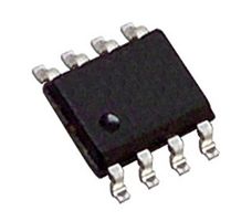
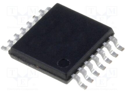
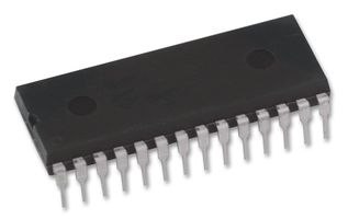
LT1376CS8-5
The LT ?
1375/LT1376 are 500kHz monolithic buck mode
switching regulators. A 1.5A switch is included on the die
along with all the necessary oscillator, control and logic
circuitry. High switching frequency allows a considerable
reduction in the size of external components. The topology
is current mode for fast transient response and good loop
stability. Both fixed output voltage and adjustable parts are
available.
LT1431IS8
The LT?1431 is an adjustable shunt voltage regulator
with 100mA sink capability, 0.4% initial reference voltage
tolerance and 0.3% typical temperature stability. On-chip
divider resistors allow the LT1431 to be configured as a
5V shunt regulator, with 1% initial voltage tolerance and
requiring no additional external components. By adding
two external resistors, the output voltage may be set to
any value between 2.5V and 36V. The nominal internal
current limit of 100mA may be decreased by including
one external resistor.
A simplified 3-pin version, the LT1431CZ/LT1431IZ, is
available for applications as an adjustable reference and
is pin compatible with the TL431.
LT1490CN8
The dual LT?
1490 and quad LT1491 op amps operate on all
single and split supplies with a total voltage of 2V to 44V
drawing only 40?A of quiescent current per amplifier. These
amplifiers are reverse supply protected; they draw no current
for reverse supply up to 18V. The input range of the LT1490/
LT1491 includes both supplies and the output swings to both
supplies. Unlike most micropower op amps, the LT1490/
LT1491 can drive heavy loads; their rail-to-rail outputs drive
20mA. The LT1490/LT1491 are unity-gain stable and drive all
capacitive loads up to 10,000pF when optional 0.22?F and
150? compensation is used.
LT1490CS8
The LT1490/LT1491 have a unique input stage that operates and remains high impedance when above the positive
supply. The inputs take 44V both differential and common
mode even when operating on a 3V supply. Built-in resistors protect the inputs for faults below the negative supply
up to 22V. There is no phase reversal of the output for inputs
22V below V? or 44V above V?, independent of V .
The LT1490 dual op amp is available in the 8-pin MSOP,
SO and PDIP packages. The quad LT1491 is available in
the 14-pin SO and PDIP packages.
LT1521IST5
Dropout Voltage: 0.5V
n Output Current: 300mA
n Quiescent Current: 12?A
n No Protection Diodes Needed
n Adjustable Output from 3.8V to 20V
n Fixed Output Voltages: 3V, 3.3V, 5V
n Controlled Quiescent Current in Dropout
n Shutdown IQ = 6?A
n Reverse Battery Protection
n No Reverse Current
n Thermal Limiting
LT1785IS8
The LT?1785/LT1791 are half-duplex and full-duplex differential bus transceivers for RS485 and RS422 applications
which feature on-chip protection from overvoltage faults
on the data transmission lines. Receiver input and driver
output pins can withstand voltage faults up to ?60V with
respect to ground with no damage to the device. Faults
may occur while the transceiver is active, shut down or
powered off.
Data rates to 250kbaud on networks of up to 128 nodes
are supported. Controlled slew rates on the driver outputscontrol EMI emissions and improve data transmission integrity on improperly terminated lines. Drivers are
specified to operate with inexpensive cables as low as
72? characteristic impedance.
The LT1785A/LT1791A devices have ?fail-safe? receiver
inputs to guarantee a receiver output high for shorted, open
or inactive data lines. On-chip ESD protection eliminates
need for external protection devices.
The LT1785/LT1785A are available in 8-lead DIP and SO
packages and the LT1791/LT1791A in 14-lead DIP and
SO packages.
LTC1040CSW#DPR
The LTC?
1040 is a monolithic CMOS dual comparator
manufactured using Linear Technology?s enhanced
LTCMOSTM silicon gate process. Extremely low operating
power levels are achieved by internally switching the
comparator ON for short periods of time. The CMOS
output logic holds the output information continuously
while not consuming any power.
In addition to switching power ON, a switched output is
provided to drive external loads during the comparator?s
active time. This allows not only low comparator power,
but low total system power.
LTC1051CN8
The LTC?
1051/LTC1053 are high performance, low cost
dual/quad zero-drift operational amplifiers. The unique
achievement of the LTC1051/LTC1053 is that they integrate
on chip the sample-and-hold capacitors usually required
externally by other chopper amplifiers. Further, the
LTC1051/LTC1053 offer better combined overall DC and
AC performance than is available from other chopper
stabilized amplifiers with or without internal sample/hold
capacitors.
The LTC1051/LTC1053 have an offset voltage of 0.5?V,
drift of 0.01?V/?C, DC to 10Hz, input noise voltage typically
1.5?VP-P and typical voltage gain of 140dB. The slew rate
of 4V/?s and gain bandwidth product of 2.5MHz are
achieved with only 1mA of supply current per op amp
LTC1487CS8
The LTC?
1487 is an ultra-low power differential line transceiver designed with high impedance inputs allowing up to
256 transceivers to share a single bus. It meets the
requirements of RS485 and RS422. The LTC1487 features
output drivers with controlled slew rate, decreasing the
EMI radiated from the RS485 lines, and improving signal
fidelity with misterminated lines. The CMOS design offers
significant power savings without sacrificing ruggedness
against overload or ESD damage. Typical quiescent current is only 80?A while operating and 1?A in shutdown
LTC1755EGN
The LTC?
1487 is an ultra-low power differential line transceiver designed with high impedance inputs allowing up to
256 transceivers to share a single bus. It meets the
requirements of RS485 and RS422. The LTC1487 features
output drivers with controlled slew rate, decreasing the
EMI radiated from the RS485 lines, and improving signal
fidelity with misterminated lines. The CMOS design offers
significant power savings without sacrificing ruggedness
against overload or ESD damage. Typical quiescent current is only 80?A while operating and 1?A in shutdown.
LTC491CS
The LTC?
491 is a low power differential bus/line transceiver designed for multipoint data transmission standard
RS485 applications with extended common mode range
(12V to ?7V). It also meets the requirements of RS422.
The CMOS design offers significant power savings over its
bipolar counterpart without sacrificing ruggedness against
overload or ESD damage.
The driver and receiver feature three-state outputs, with
the driver outputs maintaining high impedance over the
entire common mode range. Excessive power dissipation
caused by bus contention or faults is prevented by a
thermal shutdown circuit which forces the driver outputs
into a high impedance state.
The receiver has a fail safe feature which guarantees a high
output state when the inputs are left open.
Both AC and DC specifications are guaranteed from 0?C to
70?C and 4.75V to 5.25V supply voltage range.


