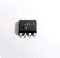
LF356H
The LF356-MIL device are the first monolithic JFET
input operational amplifiers to incorporate wellmatched, high-voltage JFETs on the same chip with
standard bipolar transistors (BI-FET? Technology).
These amplifiers feature low input bias and offset
currents/low offset voltage and offset voltage drift,
coupled with offset adjust, which does not degrade
drift or common-mode rejection. The devices are also
designed for high slew rate, wide bandwidth,
extremely fast settling time, low voltage and current
noise and a low 1/f noise corner.
LF356M
The LFx5x devices are the first monolithic JFET input
Monolithic Amplifiers operational amplifiers to incorporate well-matched,
? New Output Stage Allows Use of Large high-voltage JFETs on the same chip with standard
Capacitive Loads (5,000 pF) Without Stability bipolar transistors (BI-FET? Technology). These
Problems amplifiers feature low input bias and offset
currents/low offset voltage and offset voltage drift,
? Internal Compensation and Large Differential coupled with offset adjust, which does not degrade Input Voltage Capability drift or common-mode rejection. The devices are also
? Common Features designed for high slew rate, wide bandwidth,
? Low extremely fast settling time, low voltage and current Input Bias Current: 30 pA
noise and a low 1/f noise corne
LF398 Sample and Hold Amplifier IC DIP-8
he LF398 devices are monolithic sample-and-hold circuits that use BI-FET technology to obtain ultrahigh DC accuracy with fast acquisition of signal and low droop rate. Operating as a unity-gain follower, DC gain accuracy is 0.002% typical and acquisition time is as low as 6 ?s to 0.01%. A bipolar input stage is used to achieve low offset voltage and wide bandwidth. Input offset adjust is accomplished with a single pin and does not degrade input offset drift. The wide bandwidth allows the LF398 to be included inside the feedback loop of 1-MHz operational amplifiers without having stability problems. Input impedance of 1010 ? allows high-source impedances to be used without degrading accuracy. P-channel junction FETs are combined with bipolar devices in the output amplifier to give droop rates as low as 5 mV/min with a 1-?F hold capacitor.
LF411CD
This device is a low-cost, high-speed, JFET-input operational amplifier with very low input offset voltage and
a maximum input offset voltage drift. It requires low supply current, yet maintains a large gain-bandwidth product
and a fast slew rate. In addition, the matched high-voltage JFET input provides very low input bias and offset
currents.
The LF411 can be used in applications such as high-speed integrators, digital-to-analog converters,
sample-and-hold circuits, and many other circuits.
The LF411C is characterized for operation from 0?C to 70?C. The LF411I is characterized for operation from
?40?C to 85?C.
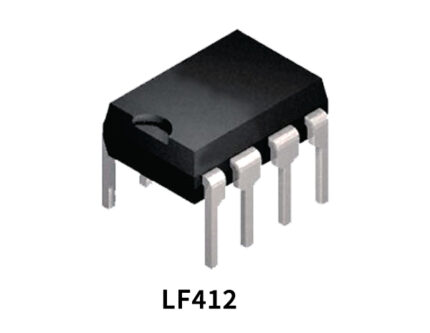
LF412 Dual JFET Input Operational Amplifier IC DIP-8
The LF412 devices are low cost, high speed, JFET input operational amplifiers with very low input offset voltage and input offset voltage drift. They require low supply current yet maintain a large gain bandwidth product and fast slew rate. In addition, well matched high voltage JFET input devices provide very low input bias and offset currents. The LF412 dual is pin compatible with the LM1558, allowing designers to immediately upgrade the overall performance of existing designs.
These amplifiers may be used in applications such as high speed integrators, fast D/A converters, sample and hold circuits and many other circuits requiring low input offset voltage and drift, low input bias current, high input impedance, high slew rate and wide bandwidth.
LF444CN
The LF444 quad low power operational amplifier 23? ? Supply Current of a LM148: 200 ?A/Amplifier
provides many of the same AC characteristics as the (max)
industry standard LM148 while greatly improving the
? Low Input Bias Current: 50 pA (max) DC characteristics of the LM148. The amplifier has
? High Gain Bandwidth: 1 MHz the same bandwidth, slew rate, and gain (10 k? load)
as the LM148 and only draws one fourth the supply ? High Slew Rate: 1 V/?s
current of the LM148. In addition the well matched
? Low Noise Voltage for Low Power 35 nV/?Hz high voltage JFET input devices of the LF444 reduce
? Low Input Noise Current 0.01 pA/?Hz the input bias and offset currents by a factor of
? High Input Impedance: 1012? 10,000 over the LM148. The LF444 also has a very
low equivalent input noise voltage for a low power
? High Gain: 50k (min) amplifier.
LKN614PN
LM101AH
The LM101A series are general purpose operational ? Improved Specifications include:
amplifiers which feature improved performance over
? Offset Voltage 3 mV Maximum Over industry standards like the LM709. Advanced
Temperature (LM101A/LM201A) processing techniques make possible an order of
? Input Current 100 nA Maximum Over magnitude reduction in input currents, and a redesign
Temperature (LM101A/LM201A) of the biasing circuitry reduces the temperature drift
of input current. ? Offset Current 20 nA Maximum Over
Temperature (LM101A/LM201A) This amplifier offers many features which make its
? Specified Drift Characteristics application nearly foolproof: Overload protection on
the input and output, no latch-up when the common
? Offsets Specified Over Entire Common Mode mode range is exceeded, and freedom from and Supply Voltage Ranges oscillations and compensation with a single 30 pF
? Slew Rate of 10V/?s as a Summing Amplifier Capacitor. It has advantages over internally
compensated amplifiers in that the frequency
compensation can be tailored to the particular
application. For example, in low frequency circuits it
can be overcompensated for increased stability
margin or the compensation can be optimized to give
more than a factor of ten improvement in high
frequency performance for most applications


