

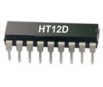
HT12D Decoder IC
₹45.00
HT12D is a decoder integrated circuit that belongs to 212 series of decoders. This series of decoders are mainly used for remote control system applications, like burglar alarm, car door controller, security system etc. It is mainly provided to interface RF and infrared circuits.? They are paired with 212 series of encoders. The chosen pair of encoder/decoder should have same number of addresses and data format.In simple terms, HT12D converts the serial input into parallel outputs. It decodes the serial addresses and data received by, say, an RF receiver, into parallel data and sends them to output data pins. The serial input data is compared with the local addresses three times continuously. The input data code is decoded when no error or unmatched codes are found. A valid transmission in indicated by a high signal at VT pin. HT12D is capable of decoding 12 bits, of which 8 are address bits and 4 are data bits. The data on 4 bit latch type output pins remain unchanged until new is received.
1000 in stock (can be backordered)
Specifications & Features of HT12D Decoder IC:-
- Operating voltage: 2.4V~12V
- Low power and high noise immunity CMOS technology
- Low standby current
- Capable of decoding 12 bits of information
- Binary address setting
- Received codes are checked 3 times
- Address/Data number combination
- HT12D: 8 address bits and 4 data bits
- Built-in oscillator needs only 5% resistor
- Valid transmission indicator
- Easy interface with an RF or an infrared transmission medium
- Minimal external components
- Pair with Holteks212 series of encoders
- 18-pin DIP
Applications of HT12D Decoder IC:-
- Burglar alarm system
- Smoke and fire alarm system
- Garage door controllers
- Car door controllers
- Car alarm system
- Security system
- Cordless telephones
- Other remote control systems


MAECENAS IACULIS
Vestibulum curae torquent diam diam commodo parturient penatibus nunc dui adipiscing convallis bulum parturient suspendisse parturient a.Parturient in parturient scelerisque nibh lectus quam a natoque adipiscing a vestibulum hendrerit et pharetra fames nunc natoque dui.
ADIPISCING CONVALLIS BULUM
- Vestibulum penatibus nunc dui adipiscing convallis bulum parturient suspendisse.
- Abitur parturient praesent lectus quam a natoque adipiscing a vestibulum hendre.
- Diam parturient dictumst parturient scelerisque nibh lectus.
Scelerisque adipiscing bibendum sem vestibulum et in a a a purus lectus faucibus lobortis tincidunt purus lectus nisl class eros.Condimentum a et ullamcorper dictumst mus et tristique elementum nam inceptos hac parturient scelerisque vestibulum amet elit ut volutpat.
Related products
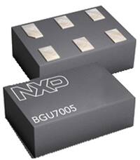
BGU7005
- Covers the entire GNSS L1 range, 1559 to 1610 MHz
- Noise figure (NF) is equal to 0.85 dB.
- Increase 16.5 dB
- A lot of input Pi(1dB), or 1 dB compression point, is 11 dBm.
- High IP3i out of band of 9 dBm
- 1.5 to 3.1 volts is the supply voltage.
- Consumption of current in power-saving mode is 1 A.
- Optimized performance at 4.5 mA, a low supply current
- Output matching that is integrated
- Only needs one supply decoupling capacitor and one input matching inductor.
- Decoupled DC input and output
- All pins have ESD protection (HBM > 2 kV).
- Temperature-stabilized bias included for simple design
- Small leadless 6-pin package 1.45 mm, 1 mm, and 0.5 mm
- Transit frequency of 110 GHz using SiGe:C technology
CC2640F128RSM
- Building and Home Automation-Appliances That Are Connected -Lights -Locks -The Gateways -Systems for Security
- Industrial- Supply chain - Manufacturing and Production - Robotics - Asset Management and Tracking - Wireless Display - Replacement of cables ? HMI - Access Management
- Retail-The beacons - Promotion - Price Tags and ESL - Payment and Point of Sale Systems
- Medical and Health-Temperature gauges - SpO2 - Blood pressure and glucose metres - Weighbridges - Vitals Tracking - Aids to hearing
- Exercise and Sports-Fitness trackers and activity monitors -Monitors for Heart Rate -Operating Sensors -Bicycle Sensors -Watches for sports - Fitness Gear - Gear for team sports
- Accessories-Toys -Followers -Tags for bags -Smartwatches
- Microcontroller-Strong ARM? Cortex? -M3 - 142 for EEMBC CoreMark? - Maximum Clock Speed of 48 MHz - 128 KB of programmable in-system flash - Cache: 8KB of SRAM - 20KB of SRAM with ultra-low leakage. - JTAG and 2-Pin cJTAG Debugging - Facilitates Over-The-Air Upgrade (OTA)
- Sensor Controller with Ultralow Power- Can Operate Independently of the Rest of the System -16-Bit architecture - 2KB of SRAM with extremely minimal leakage for code and data.
- Peripherals- Any GPIO Can Be Used to Route All Digital Peripheral Pins - Four modules for general-purpose timers. - 200 ksamples/s, 8-Channel Analog MUX, 12-Bit ADC - Comparator for Continuous Time - Ultralow-Power Analog Comparer -Modifiable Current Source - Clock in Real Time (RTC) - Security Module AES-128 -The TRNG (True Random Number Generator) (TRNG) - Depending on the package option, 10, 15, or 31 GPIOs - Eight capacitive-sensing buttons are supported. - Temperature sensor built-in


CC2650F128RHB
- Microprocessor - Strong ARM Cortex-M3 processor - 142 for EEMBC CoreMark? - Maximum Clock Speed of 48 MHz - 128 KB of programmable in-system flash - Cache: 8KB of SRAM - 20KB of SRAM with ultra-low leakage. - JTAG and 2-Pin cJTAG Debugging - Facilitates Over-The-Air Upgrade (OTA)
- Sensor Controller with Ultralow Power - Can Operate Independently of the Rest of the System - 16-Bit architecture - 2KB of SRAM with extremely minimal leakage for code and data.
- Packages Compliant with RoHS - RSM VQFN32, 4-mm x?4-mm (10 GPIOs) - RHB VQFN32, 5-mm x?5-mm (15 GPIOs) - RGZ VQFN48, 7-mm x?7-mm (31 GPIOs)
- Peripherals - Any GPIO Can Be Used to Route All Digital Peripheral Pins - Four modules for general-purpose timers. - 200 ksamples/s, 8-Channel Analog MUX, 12-Bit ADC - Comparator for Continuous Time - Ultralow-Power Analog Comparer -Modifiable Current Source - UART - Clock in Real Time (RTC) - Security Module AES-128 - The TRNG (True Random Number Generator) (TRNG) - Depending on the package option, 10, 15, or 31 GPIOs - Eight capacitive-sensing buttons are supported. - Temperature sensor built-in
- ?Outside System - Internal On-Chip DC-DC Converter - Low Number of External Components - Complete Integration With Simple LinkTM CC2590 and CC2592 Range Extenders - Compatible with the CC13xx pin of Simple Link - VQFN Packages in 4-mm x 4-mm and 5-mm x 5-mm sizes
- Small Power - Broad Supply Voltage Spectrum ? In normal use, 1.8 to 3.8 V ? 1.7 to 1.95 V in external regulator mode -5.9 mA Active-Mode RX - Active-Mode TX: 6.1 mA at 0 dBm - 9.1 mA for Active-Mode TX at +5 dBm -MCU in Active Mode: 61 A/MHz -48.5 CoreMark/mA for Active-Mode MCU -8.2 A/MHz Active-Mode Sensor Controller - RAM/CPU Retention and RTC Running: 1 A in Standby - Shutdown 100 nanoamperes (Wake Up on External Events)
- Electronics for consumers
- Cellular Phone Accessory
- Sports and exercise gear
- Applications for HID
- Building and Home Automation
- Lighting Management
- Security and Alarm
- Labeling Electronic Shelves
- Nearby tags
- Health
- Wireless controls
- Sensor Networks, Wireless

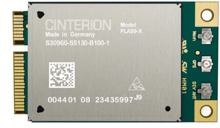
L30960-N3410-A400
- LTE (20,8,3,7,1); 3G (8,3); and 2G Dual Band PLS8-E
- PLS8-US: 3G (5,4,2), 2G Quad Band, and LTE (17,5,4,2).
- LTE (1,3,19); 3G; PLS8-J (1,19)
- PLS8-X: 3G (5,4,2), 2G Quad Band, and LTE (13,17,5,4,2).
- LTE PLS8-V: (13,4,2)
- LTE (2x2 DL-MIMO; FDD 3GPP Release 9)
- 3GPP Release 8; UMTS/HSPA (FDD); Rx diversity
- 3GPP Release 6; DARP/SAIC; GSM/GPRS/EDGE
- SIM Application Toolkit, version 99 of the 3GPP
- Using AT instructions to control (Hayes, TS 27.007, TS 27.005)
- Complete GPS/GLONASS integration (Qualcomm gpsOne Gen8A)
- 3.3 to 4.2 V supply voltage range, especially tuned for low power usage
- Dimensions are 29 mm by 33 mm by 2,2 mm (PLS8-V/-X: H=2,9 mm).
- Range of Operation: -40 ?C to +85 ?C
- EuP support, RoHS and REACH compliance
- Multiple composite modes and a Linux/Mac-compliant mode are supported by the USB interface.
- USB-based firmware update
- BIP (Bearer Independent Protocol) (Bearer Independent Protocol)
- From Rel.3.0 and for PLS8-X /-V, IP services (Client & Server, TCP/IP & UDP, Transparent & Nontransparent) are available.
- According to 3GPP TS 27.010, a multiplexer
- PLS8-X Automatic Carrier Switching

L30960-N5130-B100
- LTE (2x2 DL-MIMO; FDD 3GPP Release 9)
- 3GPP Release 8; UMTS/HSPA (FDD); Rx diversity
- 3GPP Release 6; DARP/SAIC; GSM/GPRS/EDGE
- SIM Application Toolkit, version 99 of the 3GPP
- Using AT instructions to control (Hayes, TS 27.007, TS 27.005)
- 3.3 to 4.2 V supply voltage range, especially tuned for low power usage
- Size: 40, 32, and 2,8 mm
- Range of Operation Temperature: -40 ?C to +95 ?
- Compliant with RoHS, RED, and REACH, EuP assistance
- The USB 2.0/3.0 interface provides several composite modes and a mode that is compatible with Linux and Mac.
- USB-based firmware update

MT8870 IC – DTMF Decoder IC

SKY13374-397LF
- The frequency range for broadband is 300 kHz to 6.0 GHz.
- Low insertion loss at 1 GHz and 6 GHz: 0.35 dB and 0.8 dB, respectively
- There is no need for external DC blocking capacitors.
- 1.65 to 3.0 V (VCTRL), 2.5 to 4.8 V are examples of positive low control voltages (VBATT)
- QFN (12-pin, 2 x 2 mm) small packaging (MSL1, 260 C per JEDEC J-STD-020)
- Wireless LANs with dual bands (802.11 a/b/g/n)
- Switching between diversity antennas
- WCDMA mobile phones and data cards
- SPDT switch configuration
- Frequency Minimum: 300 kHz
- 6 GHz maximum frequency
- Loss of Insertion: 0.8 dB
- Type of Off Isolation: 2 dB
- 40 C for the minimum operating temperature
- 85 C is the maximum operating temperature.
- SMD/SMT mounting style
- Technology: Si
- Packaging: Reel/ Cut Tape


Reviews
There are no reviews yet.