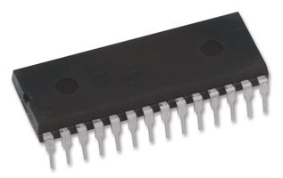
SN74HCT540N
These octal buffers and line drivers are designed to have the performance of the ?HCT240 devices and a pinout
with inputs and outputs on opposite sides of the package. This arrangement greatly facilitates printed circuit
board layout.
The 3-state control gate is a 2-input NOR. If either output-enable (OE1 or OE2) input is high, all eight outputs
are in the high-impedance state. The ?HCT540 devices provide inverted data at the outputs.
To ensure the high-impedance state during power up or power down, OE should be tied to VCC through a pullup
resistor; the minimum value of the resistor is determined by the current-sinking capability of the
SN74LS00NS
? Package Options Include:
? Plastic Small-Outline (D, NS, PS)
? Shrink Small-Outline (DB)
? Ceramic Flat (W)
? Ceramic Chip Carriers (FK)
? Standard Plastic (N)
? Ceramic (J)
? Also Available as Dual 2-Input Positive-NAND
Gate in Small-Outline (PS) Package
? Inputs Are TTL Compliant; VIH = 2 V and
VIL = 0.8 V
? Inputs Can Accept 3.3-V or 2.5-V Logic Inputs
? SN5400, SN54LS00, and SN54S00 are
Characterized For Operation Over the Full Military
Temperature Range of ?55?C to 125?C
SN74LS125AN
n
These bus buffers feature three-state outputs
that, when enabled, have the low impedance
characteristics of a TTL output with additional
drive capability at high logic levels to permit
driving heavily loaded bus lines without external
pullup resistors. When disabled, both output
transistors are turned off, presenting a
high-impedance state to the bus so the output will
act neither as a significant load nor as a driver. The
?125 and ?LS125A devices? outputs are disabled
when G is high. The ?126 and ?LS126A devices?
outputs are disabled when G is lo
SN74LS126AN
n
These bus buffers feature three-state outputs
that, when enabled, have the low impedance
characteristics of a TTL output with additional
drive capability at high logic levels to permit
driving heavily loaded bus lines without external
pullup resistors. When disabled, both output
transistors are turned off, presenting a
high-impedance state to the bus so the output will
act neither as a significant load nor as a driver. The
?125 and ?LS125A devices? outputs are disabled
when G is high. The ?126 and ?LS126A devices?
outputs are disabled when G is l


