
PIC16LF877A-I/PT
10-bit, up to 8-channel Analog-to-Digital
Converter (A/D)
? Brown-out Reset (BOR)
? Analog Comparator module with:
- Two analog comparators
- Programmable on-chip voltage reference
(VREF) module
- Programmable input multiplexing from device
inputs and internal voltage reference
- Comparator outputs are externally accessible

PIC18F458-I/PT
? 10-bit, up to 8-channel Analog-to-Digital Converter
module (A/D) with:
- Conversion available during Sleep
- Up to 8 channels available
? Analog Comparator module:
- Programmable input and output multiplexing
? Comparator Voltage Reference module
? Programmable Low-Voltage Detection (LVD) module:
- Supports interrupt-on-Low-Voltage Detection
? Programmable Brown-out Reset (BOR)
PIC18F46K20-E/ML
? Operating Voltage Range: 1.8V to 3.6V
? Self-Programmable under Software Control
? Programmable 16-Level High/Low-Voltage
Detection (HLVD) module:
- Interrupt on High/Low-Voltage Detection
? Programmable Brown-out Reset (BOR):
- With software enable option
? Extended Watchdog Timer (WDT):
- Programmable period from 4 ms to 131s
? Single-Supply 3V In-Circuit Serial
Programming? (ICSP?) via Two Pins
? In-Circuit Debug (ICD) via Two Pins
PIC18LF6627T-I/PT
? C Compiler Optimized Architecture
? 100,000 Erase/Write Cycle Enhanced Flash
Program Memory Typical
? 1,000,000 Erase/Write Cycle Data EEPROM
Memory Typical
? Flash/Data EEPROM Retention: 100 Years Typical
? Self-Programmable under Software Control
? Priority Levels for Interrupts
? 8 x 8 Single-Cycle Hardware Multiplier
? Extended Watchdog Timer (WDT):
- Programmable period from 4 ms to 131s
? Single-Supply 5V In-Circuit Serial Programming?
(ICSP?) via Two Pins
? In-Circuit Debug (ICD) via Two Pins
? Wide Operating Voltage Range: 2.0V to 5.5V
? Programmable Brown-out Reset (BOR) with
Software Enable Option

PIC24HJ32GP202T-I/SO
Core: 16-bit PIC24H CPU
? Code-efficient (C and Assembly) architecture
? Single-cycle mixed-sign MUL plus hardware divide
Clock Management
? 2% internal oscillator
? Programmable PLLs and oscillator clock sources
? Fail-Safe Clock Monitor (FSCM)
? Independent Watchdog Timer (WDT)
? Fast wake-up and start-up
Power Management
? Low-power management modes (Sleep, Idle, Doze)
? Integrated Power-on Reset and Brown-out Reset
? 1.35 mA/MHz dynamic current (typical)
? 55 ?A IPD current (typical)
Advanced Analog Features
? ADC module:
- Configurable as 10-bit, 1.1 Msps with four
S&H or 12-bit, 500 ksps with one S&H
- Ten analog inputs on 28-pin devices and up
to 13 analog inputs on 44-pin devices
? Flexible and independent ADC trigger sources
PIC24HJ64GP502T-QFN-28
? 10/12-bit ADC with 1.1Msps/500 ksps conversion
rate:
- Up to 13 ADC input channels and four S&H
- Flexible/Independent trigger sources
? 150 ns Comparators:
- Up to two Analog Comparator modules
- 4-bit DAC with two ranges for Analog Comparators
? Parallel Master Port (PMP)
? Two UART modules (10 Mbps)
- Supports LIN 2.0 protocols
- RS-232, RS-485, and IrDA? support
? Two 4-wire SPI modules (15 Mbps)
? Enhanced CAN (ECAN) module (1 Mbaud) with
2.0B support
? I2C module (100K, 400K and 1Mbaud) with
SMBus support
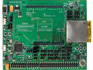
QCA4020-0-217MSP-TR-0D-0
Features of QCA4020
- The QCA4020 tri-mode SoC combines 802.15.4, dual-band Wi-Fi, and Bluetooth 5 technologies.
- Low power, isolated 15.4 SW MAC, 15.4 and BLE drivers, coex management, and Wi-Fi operations processors (QCA4020 only)
- Secure boot, trusted execution environments, encrypted storage, key provisioning, and wireless protocol security are all features of cutting-edge hardware-based security.
- a full range of interfaces and peripherals, including SPI, UART, PWM, I2S, I2C, SDIO, ADC, and GPIOs.
- Low power sensor use cases are made possible by an integrated sensor hub for post-processing.
- Reduced package size enables improved form factors.
- Package Type - 11.2 x 11.2mm, 0.65mm pitch, 217-ball BGA (QCA4020)
- Application CPU : 1. Arm Cortex-M4F @ up to 128MHz 2. 32KB- L1 cache controller, XIP from external S-flash 3. Internal Memory: 300+KB RAM reserved for applications
- Connectivity/System CPU : 1. Dedicated processor for Bluetooth LE LC and 15.4 MAC 2. Dedicated processor for 802.11 a/b/g/n 3. Isolated Memory: RAM, ROM
- Low Power Bluetooth & 15.4 (Separate radios) : 1. Bluetooth v5.0, PA =+4dBm/+10dBm (for Long Range) 2. 802.15.4: 2006 compliant, 15.4e, 2.4GHz DSSS 3. +4dBm/+21dBm (for Long Range)
- Wi-Fi (QCA4020 only) : Dual Band, 1x1, HT20, MCS0-7, 2.4/5GHz, PA=+18dBm
- Sensor Hub : Low power HW+App CPU, Interface: I2C, SPI, ADC
- Display : Segmented or character display with SPI or I2C interfaces
- Interfaces : 1. 2C, UART, SPI/Q-SPI, ADC (8ch, 12-bit 1Msps) 2. PWM, SDIO2.0, USB2.0 HS, I2S, GPIOs
- Security 1. Secure boot, Secure Storage, HW Crypto Engine 2. HW ECC, 16-bit true random number generator 3. Trusted Execution Environment
- Direct Battery Connection : 1.8V-3.6V