
PIC16F819 Microcontroller
The PIC16F819 is a 18/20-Pin Enhanced Flash Microcontrollers with nano Watt Technology. The following are the features:-
? 16 I/O pins with individual direction control
? High sink/source current: 25 mA
? Timer0: 8-bit timer/counter with 8-bit prescaler
? Timer1: 16-bit timer/counter with prescaler, can be incremented during Sleep via external crystal/clock
? Timer2: 8-bit timer/counter with 8-bit period register, prescaler and postscaler
? Capture, Compare, PWM (CCP) module:
- Capture is 16-bit, max. resolution is 12.5 ns
- Compare is 16-bit, max. resolution is 200 ns
- PWM max. resolution is 10-bit
? 10-bit, 5-channel Analog-to-Digital converter

PIC16F819-I/P

PIC16F84A Microcontroller
The PIC16F84A ?is a 18-pin Enhanced FLASH/EEPROM 8-Bit Microcontroller. The following are the features:-
? 13 I/O pins with individual direction control
? High current sink/source for direct LED drive
- 25 mA sink max. per pin
- 25 mA source max. per pin
? TMR0: 8-bit timer/counter with 8-bit programmable prescaler
PIC16F84A-04I/P
All PIC? microcontrollers employ an advanced RISC
architecture. PIC16F8X devices have enhanced core
features, eight-level deep stack, and multiple internal
and external interrupt sources. The separate
instruction and data buses of the Harvard architecture
allow a 14-bit wide instruction word with a separate
8-bit wide data bus. The two stage instruction pipeline
allows all instructions to execute in a single cycle,
except for program branches (which require two
cycles). A total of 35 instructions (reduced instruction
set) are available. Additionally, a large register set is
used to achieve a very high performance level.
PIC16F8X microcontrollers typically achieve a 2:1 code
compression and up to a 4:1 speed improvement (at 20
MHz) over other 8-bit microcontrollers in their class.

PIC16F870 Microcontroller
he PIC16F870 ?is a 28/40-Pin, 8-Bit CMOS FLASH Microcontrollers. The following are the features:-
? Timer0: 8-bit timer/counter with 8-bit prescaler
? Timer1: 16-bit timer/counter with prescaler, can be incremented during SLEEP via external crystal/clock
? Timer2: 8-bit timer/counter with 8-bit period register, prescaler and postscaler
? One Capture, Compare, PWM module
- Capture is 16-bit, max. resolution is 12.5 ns
- Compare is 16-bit, max. resolution is 200 ns
- PWM max. resolution is 10-bit
? 10-bit multi-channel Analog-to-Digital converter
? Universal Synchronous Asynchronous Receiver Transmitter (USART/SCI) with 9-bit address detection
? Parallel Slave Port (PSP) 8-bits wide, with external RD, WR and CS controls (40/44-pin only)
? Brown-out detection circuitry for Brown-out Reset (BOR)

PIC16F870-I/SP

PIC16F871-20I/SP

PIC16F873A Microcontroller
The PIC16F873A?is a 28/40/44-Pin Enhanced Flash Microcontrollers . The following are the features:-
? Timer0: 8-bit timer/counter with 8-bit prescaler
? Timer1: 16-bit timer/counter with prescaler, can be incremented during SLEEP via external crystal/clock
? Timer2: 8-bit timer/counter with 8-bit period register, prescaler and postscaler
? One Capture, Compare, PWM module
- Capture is 16-bit, max. resolution is 12.5 ns
- Compare is 16-bit, max. resolution is 200 ns
- PWM max. resolution is 10-bit
? 10-bit multi-channel Analog-to-Digital converter
? Universal Synchronous Asynchronous Receiver Transmitter (USART/SCI) with 9-bit address detection
? Parallel Slave Port (PSP) 8-bits wide, with external RD, WR and CS controls (40/44-pin only)
? Brown-out detection circuitry for Brown-out Reset (BOR)

PIC16F873A-I/SP
PIC16F873A/876A devices are available only in 28-pin
packages, while PIC16F874A/877A devices are available in 40-pin and 44-pin packages. All devices in the
PIC16F87XA family share common architecture with
the following differences:
? The PIC16F873A and PIC16F874A have one-half
of the total on-chip memory of the PIC16F876A
and PIC16F877A
? The 28-pin devices have three I/O ports, while the
40/44-pin devices have five
? The 28-pin devices have fourteen interrupts, while
the 40/44-pin devices have fifteen
? The 28-pin devices have five A/D input channels,
while the 40/44-pin devices have eight
? The Parallel Slave Port is implemented only on
the 40/44-pin devices

PIC16F874A Microcontroller
The PIC16F874A?is a 28/40/44-Pin Enhanced Flash Microcontrollers. The following are the features:-
? Timer0: 8-bit timer/counter with 8-bit prescaler
? Timer1: 16-bit timer/counter with prescaler, can be incremented during Sleep via external crystal/clock
? Timer2: 8-bit timer/counter with 8-bit period register, prescaler and postscaler
? Two Capture, Compare, PWM modules
- Capture is 16-bit, max. resolution is 12.5 ns
- Compare is 16-bit, max. resolution is 200 ns
- PWM max. resolution is 10-bit
? Synchronous Serial Port (SSP) with SPI (Master mode) and I2C? (Master/Slave)
Universal Synchronous Asynchronous Receiver Transmitter (USART/SCI) with 9-bit address detection
? Parallel Slave Port (PSP) ? 8 bits wide with external RD, WR and CS controls (40/44-pin only)
? Brown-out detection circuitry for Brown-out Reset (BOR)

PIC16F876A-I/SP
PIC16F873A/876A devices are available only in 28-pin
packages, while PIC16F874A/877A devices are available in 40-pin and 44-pin packages. All devices in the
PIC16F87XA family share common architecture with
the following differences:
? The PIC16F873A and PIC16F874A have one-half
of the total on-chip memory of the PIC16F876A
and PIC16F877A
? The 28-pin devices have three I/O ports, while the
40/44-pin devices have five
? The 28-pin devices have fourteen interrupts, while
the 40/44-pin devices have fifteen
? The 28-pin devices have five A/D input channels,
while the 40/44-pin devices have eight
? The Parallel Slave Port is implemented only on
the 40/44-pin devices
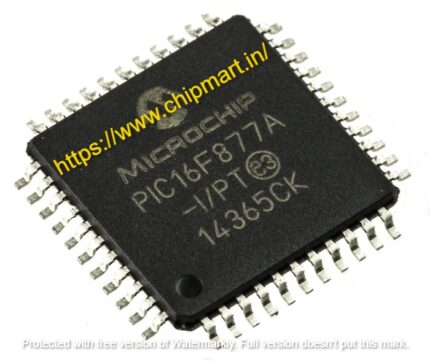
Pic16f877 I/Pt
The PIC16F873, PIC16F874, PIC16F876 and PIC16F877 are the four covered devices. Devices for the PIC16F876/873 and PIC16F877/874 available in 28-pin and 40-pin packages, respectively. On 28-pin devices, the Parallel Slave Port is not implemented. Each PIC16F87X device has the ability to access an 8K word block of program memory continuously. Only 11 bits of address are provided by the CALL and GOTO instructions, allowing branching inside any 2K program memory page. PCLATH4:3> provides the upper 2 bits of the address when performing a CALL or GOTO instruction. The user must make sure that the page choose bits are set when performing a CALL or GOTO instruction in order for the chosen programme memory page to be addressed. The full 13-bit PC is popped off the stack whenever a return from a CALL instruction (or interrupt) is performed. Therefore, the return instructions do not need the modification of the PCLATH4:3> bits (which POPs the address from the stack).
Data Memory Organization
The General Purpose Registers and Special Function Registers are divided up into several banks in the data memory. The bank select bits are bits RP1 (Status:6) and RP0 (Status:5). Each bank stretches to 7Fh (128 bytes). The Special Function Registers are only permitted in the bottom positions of each bank. General Purpose Registers, which are implemented as static RAM, are located above the Special Function Registers. Special Function Registers are present in all installed banks. For code reduction and faster access, some commonly used Special Function Registers from one bank may be duplicated in another bank.


