
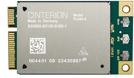
L30960-N3410-A400
Features of L30960-N3410-A400
- LTE (20,8,3,7,1); 3G (8,3); and 2G Dual Band PLS8-E
- PLS8-US: 3G (5,4,2), 2G Quad Band, and LTE (17,5,4,2).
- LTE (1,3,19); 3G; PLS8-J (1,19)
- PLS8-X: 3G (5,4,2), 2G Quad Band, and LTE (13,17,5,4,2).
- LTE PLS8-V: (13,4,2)
- LTE (2x2 DL-MIMO; FDD 3GPP Release 9)
- 3GPP Release 8; UMTS/HSPA (FDD); Rx diversity
- 3GPP Release 6; DARP/SAIC; GSM/GPRS/EDGE
- SIM Application Toolkit, version 99 of the 3GPP
- Using AT instructions to control (Hayes, TS 27.007, TS 27.005)
- Complete GPS/GLONASS integration (Qualcomm gpsOne Gen8A)
- 3.3 to 4.2 V supply voltage range, especially tuned for low power usage
- Dimensions are 29 mm by 33 mm by 2,2 mm (PLS8-V/-X: H=2,9 mm).
- Range of Operation: -40 ?C to +85 ?C
- EuP support, RoHS and REACH compliance
- Multiple composite modes and a Linux/Mac-compliant mode are supported by the USB interface.
- USB-based firmware update
- BIP (Bearer Independent Protocol) (Bearer Independent Protocol)
- From Rel.3.0 and for PLS8-X /-V, IP services (Client & Server, TCP/IP & UDP, Transparent & Nontransparent) are available.
- According to 3GPP TS 27.010, a multiplexer
- PLS8-X Automatic Carrier Switching

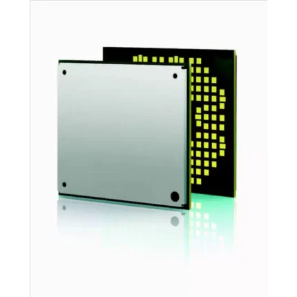
L30960-N5130-B100
Features? of? L30960-N5130-B100
- LTE (2x2 DL-MIMO; FDD 3GPP Release 9)
- 3GPP Release 8; UMTS/HSPA (FDD); Rx diversity
- 3GPP Release 6; DARP/SAIC; GSM/GPRS/EDGE
- SIM Application Toolkit, version 99 of the 3GPP
- Using AT instructions to control (Hayes, TS 27.007, TS 27.005)
- 3.3 to 4.2 V supply voltage range, especially tuned for low power usage
- Size: 40, 32, and 2,8 mm
- Range of Operation Temperature: -40 ?C to +95 ?
- Compliant with RoHS, RED, and REACH, EuP assistance
- The USB 2.0/3.0 interface provides several composite modes and a mode that is compatible with Linux and Mac.
- USB-based firmware update
L6219 Stepper Motor Driver IC DIP-24 Package


LDK220M33R 200 mA low quiescent current

LDK220M36R Voltage Regulators 200 mA

LF351 Wide Bandwidth JFET Input Op-Amp IC DIP-8
The LF351 is a low cost high speed JFET input operational amplifier with an internally trimmed input offset voltage (BI-FET IITM technology). The device requires a low supply current and yet maintains a large gain bandwidth product and a fast slew rate. In addition, well matched high voltage JFET input devices provide very low input bias and offset currents. The LF351 is pin compatible with the standard LM741 and uses the same offset voltage adjustment circuitry. This feature allows designers to immediately upgrade the overall performance of existing LM741 designs. The LF351 may be used in applications such as high speed integrators, fast D/A converters, sample-and-hold circuits and many other circuits requiring low input offset voltage, low input bias current, high input impedance, high slew rate and wide bandwidth

LF353 Wide Bandwidth Dual JFET Input Op-Amp IC DIP-8 Package
This LF353 device is a low-cost, high-speed, JFET input operational amplifier with very low input offset voltage. It requires low supply current yet maintains a large gain-bandwidth product and a fast slew rate. In addition, the matched high-voltage JFET input provides very low input bias and offset currents. The LF353 can be used in applications such as high speed integrators, digital-to-analog converters, sample-and-hold circuits, and many other circuits. The LF353 is characterized for operation from 0?C to 70?C.
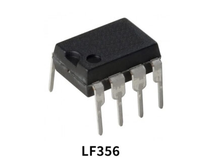
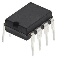
LF356 JFET Input Op-Amp IC DIP-8
The LF356 device are the first monolithic JFET input operational amplifiers to incorporate well matched, high-voltage JFETs on the same chip with standard bipolar transistors (BI-FET? Technology). These amplifiers feature low input bias and offset currents/low offset voltage and offset voltage drift, coupled with offset adjust, which does not degrade drift or common-mode rejection. The devices are also designed for high slew rate, wide bandwidth, extremely fast settling time, low voltage and current noise and a low 1/f noise corner.

LF398 Sample and Hold Amplifier IC DIP-8
he LF398 devices are monolithic sample-and-hold circuits that use BI-FET technology to obtain ultrahigh DC accuracy with fast acquisition of signal and low droop rate. Operating as a unity-gain follower, DC gain accuracy is 0.002% typical and acquisition time is as low as 6 ?s to 0.01%. A bipolar input stage is used to achieve low offset voltage and wide bandwidth. Input offset adjust is accomplished with a single pin and does not degrade input offset drift. The wide bandwidth allows the LF398 to be included inside the feedback loop of 1-MHz operational amplifiers without having stability problems. Input impedance of 1010 ? allows high-source impedances to be used without degrading accuracy. P-channel junction FETs are combined with bipolar devices in the output amplifier to give droop rates as low as 5 mV/min with a 1-?F hold capacitor.
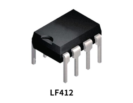
LF412 Dual JFET Input Operational Amplifier IC DIP-8
The LF412 devices are low cost, high speed, JFET input operational amplifiers with very low input offset voltage and input offset voltage drift. They require low supply current yet maintain a large gain bandwidth product and fast slew rate. In addition, well matched high voltage JFET input devices provide very low input bias and offset currents. The LF412 dual is pin compatible with the LM1558, allowing designers to immediately upgrade the overall performance of existing designs.
These amplifiers may be used in applications such as high speed integrators, fast D/A converters, sample and hold circuits and many other circuits requiring low input offset voltage and drift, low input bias current, high input impedance, high slew rate and wide bandwidth.