25AA320-I/SN
₹60.00
The Microchip Technology Inc. 25AA320/25LC320/25C320 (25XX320*) serial Electrically Erasable PROMs are 32 Kbit. A basic Serial Peripheral Interface (SPI) compliant serial bus is used to access the memory. A clock input (SCK) is required, as well as separate data in (SI) and data out (SO) lines. A Chip Selection (CS) input controls access to the device. The hold pin allows you to suspend communication with the gadget (HOLD). Transitions on the device’s inputs will be ignored while it is stopped, excluding Chip Select, enabling the host to service higher priority interrupts.
Features
? CMOS Low-Power Technology:
– Maximum write current: 3 mA
– Typical read current: 500 A
– Typical standby current: 500 nA
? 4096 x 8 Bit Storage
? 32 bytes each page
? Maximum Write Cycle Time: 5 ms
? Erase and write cycles that are self-timed
? Write Block Protection:
– Protect none, 1/4, 1/2, or the entire array.
? Integrated Write Protection:
– Data protection circuitry that is switched on and off
? Latch for write enable
– A write-protection pin
? Read in Sequence
? High dependability:
– Endurance: 1 million E/W cycles
– Data retention: more than 200 years
– ESD protection: more than 4000V
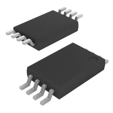
? PDIP, SOIC, and TSSOP packages with 8 pins
? TSSOP Package with 14 Leads


MAECENAS IACULIS
Vestibulum curae torquent diam diam commodo parturient penatibus nunc dui adipiscing convallis bulum parturient suspendisse parturient a.Parturient in parturient scelerisque nibh lectus quam a natoque adipiscing a vestibulum hendrerit et pharetra fames nunc natoque dui.
ADIPISCING CONVALLIS BULUM
- Vestibulum penatibus nunc dui adipiscing convallis bulum parturient suspendisse.
- Abitur parturient praesent lectus quam a natoque adipiscing a vestibulum hendre.
- Diam parturient dictumst parturient scelerisque nibh lectus.
Scelerisque adipiscing bibendum sem vestibulum et in a a a purus lectus faucibus lobortis tincidunt purus lectus nisl class eros.Condimentum a et ullamcorper dictumst mus et tristique elementum nam inceptos hac parturient scelerisque vestibulum amet elit ut volutpat.
Related products
24C32 32K bit

24LC256-I/SN

AT24CO2
AT24CO4
AT25640B-SSHL-T

M24128-DRDW8TP/K
- Support for all I2C bus modes? 1 MHz/ 400 kHz/ 100 kHz
- Memory bank- An EEPROM with 128 Kbits (16 Kbytes)
- Page Size in Bytes: 64
- In addition Make a locked page.
- Wider range of temperatures and voltages?40 to 105 degrees Celsius; 1.7 to 5.5 volts
- Schmitt trigger inputs are used to filter noise.
- Cycle time for short writes- Byte Write in 4 milliseconds- Page Write in 4 milliseconds
- Express cycling stamina. -4,000,000 Write Cycles at 25 ?C, - 1,2,000,000 Write cycles at 85 ?C & ? 900 k Cycles of writing at 105 ?C
- Data storage- at 105 ?C for more than 50 years., 200 yr at 55 ?C
- ESD Defense (Human Body Model)? 4000 V
- Packing is- Halogen-free and RoHS compliant
- SMD/SMT mounting style
- Case/Package: TSSOP-8
- Interface types: I2C and 2-Wire
- Size of Memory: 128 kbit
- Arrangement: 16 k x 8
- Minimum Supply Voltage: 1.7 V
- Maximum Supply Voltage: 5.5 V
- 40 C for the minimum operating temperature
- 105 C is the maximum operating temperature.
- 1 MHz is the maximum clock frequency.
- Time to Access: 450 ns
- Retention of Data: 200 Years
- Maximum Supply Current: 2 mA
- The M24128-DRD series
- mandatory requirement: AEC-Q100
- Packaging: Cut Tape and Reel
- Maximum Active Read Current: 2 mA
- STMicroelectronics is a brand.
- 2 mA is the operating supply current.
- Voltage Range for Operating Supply: 1.8 to 5.5 V
- Type of Product: EEPROM


M25P40-VMN6TPB
- ?4 Mbit of Flash memory
- ?2.3 V to 3.6 V single supply voltage
- ?SPI bus compatible serial interface
- ?75 MHz clock rate (maximum)
- ?Page Program (up to 256 bytes) in 0.8 ms (typical)
- ?Sector Erase (512 Kbit) in 0.6 s (typical)
- ?Bulk Erase (4 Mbit) in 4.5 s (typical)
- ?Deep Power-down mode 1 ?A (typical)
- ?Hardware Write Protection: protected area size defined by three non-volatile bits (BP0, BP1 and BP2)
- ?Electronic signatures ? JEDEC standard two-byte signature (2013h) ? Unique ID code (UID) with 16 bytes read only, available upon customer request ? RES instruction, one-byte, signature (12h), for backward compatibility
- ?Packages ? RoHS compliant
- ?Automotive grade parts available
- Memory Size -
- Supply Voltage - Min: 2.3 V
- Supply Voltage - Max: 3.6 V
- Active Read Current - Max: 8 mA
- Interface Type: SPI
- Maximum Clock Frequency: 75 MHz
- Organisation: 512 k x 8
- Data Bus Width: 8 bit
- Timing Type: Synchronous
- Minimum Operating Temperature: - 40 C
- Maximum Operating Temperature: + 85 C
- Packaging: Reel / Cut Tape
- Memory Type: NOR
- Product Type: NOR Flash
- Speed: 75 MHz


W25Q16JV-SSIQ
- SpiFlash Memories' New Family - 16M-bit/ 2M-byte W25Q16JV - Common SPI: CLK, /CS, DI, and DO - CLK, /CS, IO0, IO1 and Dual SPI - CLK, /CS, IO0, IO1, IO2, IO3 for Quad SPI. - Hardware and Software Reset
- Best Serial Flash Performance - Single, Dual, and Quad SPI clocks at 133 MHz - Dual/Quad SPI equal to 266/532MHz - Continuous data transfer rate of 66 MB/S - No fewer than 100K Program-Erase cycles per sector - Retention of data for more than 20 years
- A productive "Continuous Read" - Constant Read with 8/16/32/64-Byte Wrap - Address memory with as few as 8 clocks - Facilitates real XIP (execute in place) operation - Performs better than X16 Parallel Flash
- Wide temperature range, low power - Single 2.7 to 3.6 volt supply - Operating range: -40 to +85 ?C. - Operating temperature range: -40 to +105 ?C. - Power-down, 1A.
- 4KB sectors and flexible architecture - 4K/32K/64K-Byte Uniform Sector/Block Erase - Programmable pages can hold up to 256 bytes. - Delete/Suspend/Resume Program
- Features of Advanced Security - Write-Protect in Software and Hardware - Lock-Down Power Supply and - Extraordinary OTP security - Protection for the top/bottom and complement arrays - Protection for individual blocks and sectors - Each device has a 64-Bit unique ID. - Register for Discoverable Parameters (SFDP) - OTP locks on 3X256-Byte Security Registers - Bits in the Volatile & Non-Volatile Status Register
- Effective Packaging for Space - 8-pin SOIC 150/208 mils - USON 8-pad 2X3mm/4X3mm - XSON 8-pad 4x4-mm - WSON 8-pad 6x5-mm ? 8-ball WLCSP - For KGD and additional alternatives, contact Winbond


Reviews
There are no reviews yet.